ZHCSAJ4D November   2012  – September 2019 ADS1018

PRODUCTION DATA.  

  1. 特性
  2. 应用
  3. 说明
    1.     Device Images
      1.      K 型热电偶测量使用集成温度传感器进行冷结点补偿
  4. 修订历史记录
  5. Device Comparison Table
  6. Pin Configuration and Functions
    1.     Pin Functions
  7. Specifications
    1. 7.1 Absolute Maximum Ratings
    2. 7.2 ESD Ratings
    3. 7.3 Recommended Operating Conditions
    4. 7.4 Thermal Information
    5. 7.5 Electrical Characteristics
    6. 7.6 Timing Requirements: Serial Interface
    7. 7.7 Switching Characteristics: Serial Interface
    8. 7.8 Typical Characteristics
  8. Detailed Description
    1. 8.1 Overview
    2. 8.2 Functional Block Diagram
    3. 8.3 Feature Description
      1. 8.3.1 Multiplexer
      2. 8.3.2 Analog Inputs
      3. 8.3.3 Full-Scale Range (FSR) and LSB Size
      4. 8.3.4 Voltage Reference
      5. 8.3.5 Oscillator
      6. 8.3.6 Temperature Sensor
        1. 8.3.6.1 Converting from Temperature to Digital Codes
        2. 8.3.6.2 Converting from Digital Codes to Temperature
    4. 8.4 Device Functional Modes
      1. 8.4.1 Reset and Power-Up
      2. 8.4.2 Operating Modes
        1. 8.4.2.1 Single-Shot Mode and Power-Down
        2. 8.4.2.2 Continuous-Conversion Mode
      3. 8.4.3 Duty Cycling for Low Power
    5. 8.5 Programming
      1. 8.5.1 Serial Interface
      2. 8.5.2 Chip Select (CS)
      3. 8.5.3 Serial Clock (SCLK)
      4. 8.5.4 Data Input (DIN)
      5. 8.5.5 Data Output and Data Ready (DOUT/DRDY)
      6. 8.5.6 Data Format
      7. 8.5.7 Data Retrieval
        1. 8.5.7.1 32-Bit Data Transmission Cycle
        2. 8.5.7.2 16-Bit Data Transmission Cycle
    6. 8.6 Register Maps
      1. 8.6.1 Conversion Register [reset = 0000h]
        1. Table 4. Conversion Register Field Descriptions
      2. 8.6.2 Config Register [reset = 058Bh]
        1. Table 5. Config Register Field Descriptions
  9. Application and Implementation
    1. 9.1 Application Information
      1. 9.1.1 Serial Interface Connections
      2. 9.1.2 GPIO Ports for Communication
      3. 9.1.3 Analog Input Filtering
      4. 9.1.4 Single-Ended Inputs
      5. 9.1.5 Connecting Multiple Devices
      6. 9.1.6 Pseudo Code Example
    2. 9.2 Typical Application
      1. 9.2.1 Design Requirements
      2. 9.2.2 Detailed Design Procedure
      3. 9.2.3 Application Curves
  10. 10Power Supply Recommendations
    1. 10.1 Power-Supply Sequencing
    2. 10.2 Power-Supply Decoupling
  11. 11Layout
    1. 11.1 Layout Guidelines
    2. 11.2 Layout Example
  12. 12器件和文档支持
    1. 12.1 文档支持
      1. 12.1.1 相关文档
    2. 12.2 接收文档更新通知
    3. 12.3 社区资源
    4. 12.4 商标
    5. 12.5 静电放电警告
    6. 12.6 Glossary
  13. 13机械、封装和可订购信息

Typical Characteristics

at TA = 25°C, VDD = 3.3 V, and FSR = ±2.048 V (unless otherwise noted)
ADS1018 tc_ivdd-tmp_bas526.gif
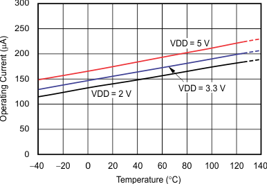
Figure 2. Operating Current vs Temperature
ADS1018 tc_oerr_1end-tmp_bas526.gif
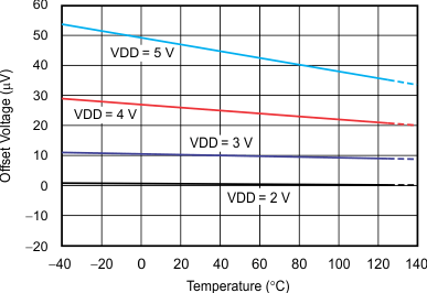
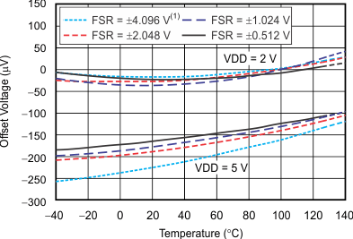
Figure 4. Single-Ended Offset Voltage vs Temperature
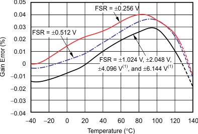
ADS1018 tc_gerr-tmp_bas526.gif
Figure 6. Gain Error vs Temperature
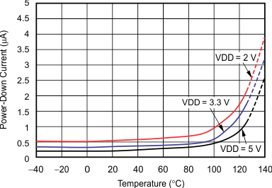
ADS1018 tc_sdown_cur-tmp_bas526.gif
Figure 3. Power-Down Current vs Temperature
ADS1018 tc_diff_oset-tmp_bas526.gif
Figure 5. Differential Offset Voltage vs Temperature
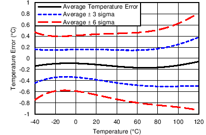
ADS1018 tc_temp_sensor_error_bas526.png
Figure 7. Temperature Sensor Error vs Temperature
This parameter expresses the full-scale range of the ADC scaling. In no event should more than VDD + 0.3 V be applied to this device.