ZHCSAK8J December 2003 – June 2022 TPS40054 , TPS40055 , TPS40057
PRODUCTION DATA
- 1 特性
- 2 应用
- 3 说明
- 4 Revision History
- 5 Pin Configuration and Functions
- 6 Specifications
-
7 Detailed Description
- 7.1 Overview
- 7.2 Functional Block Diagram
- 7.3
Feature Description
- 7.3.1 Setting the Switching Frequency (Programming the Clock Oscillator)
- 7.3.2 Programming The Ramp Generator Circuit
- 7.3.3 UVLO Operation
- 7.3.4 BP5 and BP10 Internal Voltage Regulators
- 7.3.5 Programming Soft Start
- 7.3.6 Programming Current Limit
- 7.3.7 Synchronizing to an External Supply
- 7.3.8 Loop Compensation
- 7.4 Device Functional Modes
-
8 Application and Implementation
- 8.1 Application Information
- 8.2
Typical Application
- 8.2.1 Design Requirements
- 8.2.2
Detailed Design Procedure
- 8.2.2.1 Calculate Maximum and Minimum Duty Cycles
- 8.2.2.2 Select Switching Frequency
- 8.2.2.3 Select ΔI
- 8.2.2.4 Calculate the High-Side MOSFET Power Losses
- 8.2.2.5 Calculate Synchronous Rectifier Losses
- 8.2.2.6 Calculate the Inductor Value
- 8.2.2.7 Set the Switching Frequency
- 8.2.2.8 Program the Ramp Generator Circuit
- 8.2.2.9 Calculate the Output Capacitance (CO)
- 8.2.2.10 Calculate the Soft-Start Capacitor (CSS/SD)
- 8.2.2.11 Calculate the Current Limit Resistor (RILIM)
- 8.2.2.12 Calculate Loop Compensation Values
- 8.2.2.13 Calculate the Boost and BP10V Bypass Capacitance
- 8.2.3 Application Curves
- 9 Power Supply Recommendations
- 10Layout
- 11Device and Documentation Support
- 12Mechanical, Packaging, and Orderable Information
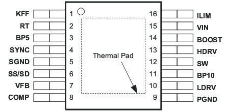
5 Pin Configuration and Functions

A. For more information on the PWP
package, refer to the PowerPAD™ Thermally Enhanced
Package application report.
B. A PowerPAD heat slug must be
connected to SGND (pin 5) or electrically isolated from all other pins.
Figure 5-1 16-Pin PWP HTSSOP Package (Top
View)Table 5-1 Pin Functions
| PIN | I/O | DESCRIPTION | |
|---|---|---|---|
| NAME | NO. | ||
| BOOST | 14 | O | Gate drive voltage for the high side N-channel MOSFET. The BOOST voltage is 9 V greater than the SW voltage. Connect a 0.1-µF ceramic capacitor from this pin to the drain of the lower MOSFET. |
| BP5 | 3 | O | 5-V reference. Bypass this pin to ground with a 0.1-µF ceramic capacitor. This pin can be used with an external DC load of 1 mA or less. |
| BP10 | 11 | O | 10-V reference used for gate drive of the N-channel synchronous rectifier. Bypass this pin with a 1-µF ceramic capacitor. This pin can be used with an external DC load of 1 mA or less. |
| COMP | 8 | O | Output of the error amplifier and input to the PWM comparator. A feedback network is connected from this pin to the VFB pin to compensate the overall loop. The COMP pin is internally clamped above the peak of the ramp to improve large signal transient response. |
| HDRV | 13 | O | Floating gate drive for the high-side N-channel MOSFET. This pin switches from BOOST (MOSFET on) to SW (MOSFET off). |
| ILIM | 16 | I | Current limit pin. Used to set the overcurrent threshold. An internal current sink from this pin to ground sets a voltage drop across an external resistor connected from this pin to VCC. The voltage on this pin is compared to the voltage drop (VIN – SW) across the high-side MOSFET during conduction. |
| KFF | 1 | I | A resistor is connected from this pin to VIN to program the amount of voltage feedforward and UVLO level. The current fed into this pin is internally divided and used to control the slope of the PWM ramp. |
| LDRV | 10 | O | Gate drive for the N-channel synchronous rectifier. This pin switches from BP10 (MOSFET on) to ground (MOSFET off). |
| PGND | 9 | Power ground reference for the device. There should be a low-impedance path from this pin to the source or sources of the lower MOSFET or MOSFETs. | |
| RT | 2 | I | A resistor is connected from this pin to ground to set the internal oscillator and switching frequency. |
| SGND | 5 | — | Signal ground reference for the device |
| SS/SD | 6 | I | Soft-start programming and shutdown pin. A capacitor connected from this pin to ground programs the soft-start time. The capacitor is charged with an internal current source of 2.3 µA. The resulting voltage ramp on the SS/SD pin is used as a second non-inverting input to the error amplifier. The output voltage begins to rise when VSS/SD is approximately 0.85 V. The output continues to rise and reaches regulation when VSS/SD is approximately 1.55 V. The controller is considered shut down when VSS/SD is 125 mV or less. The internal circuitry is enabled when VSS/SD is 210 mV or greater. When VSS/SD is less than approximately 0.85 V, the outputs cease switching and the output voltage (VO) decays while the internal circuitry remains active. |
| SW | 12 | I | This pin is connected to the switched node of the converter and used for overcurrent sensing. The TPS40054 also uses this pin for zero current sensing. |
| SYNC | 4 | I | Synchronization input for the device. This pin can be used to synchronize the oscillator to an external controller frequency. If synchronization is not used, connect this pin to SGND. |
| VFB | 7 | I | Inverting input to the error amplifier. In normal operation, the voltage on this pin is equal to the internal reference voltage, 0.7 V. |
| VIN | 15 | I | Supply voltage for the device |