ZHCSAM1F December   2012  – December 2017 TPS7A66-Q1 , TPS7A69-Q1

PRODUCTION DATA.  

  1. 特性
  2. 应用
  3. 说明
    1.     Device Images
      1.      硬件启用选项
      2.      输入电压感测选项
  4. 修订历史记录
  5. Pin Configuration and Functions
    1.     Pin Functions
  6. Specifications
    1. 6.1 Absolute Maximum Ratings
    2. 6.2 ESD Ratings
    3. 6.3 Recommended Operating Conditions
    4. 6.4 Thermal Information
    5. 6.5 Electrical Characteristics
    6. 6.6 Switching Characteristics
    7. 6.7 Typical Characteristics
  7. Detailed Description
    1. 7.1 Overview
    2. 7.2 Functional Block Diagrams
    3. 7.3 Feature Description
      1. 7.3.1 Enable (EN)
      2. 7.3.2 Regulated Output (VOUT)
      3. 7.3.3 Power-On Reset (PG)
      4. 7.3.4 Reset Delay Timer (CT)
      5. 7.3.5 Sense Comparator (SI and SO for TPS7A69-Q1)
      6. 7.3.6 Adjustable Output Voltage (FB for TPS7A6601-Q1)
      7. 7.3.7 Undervoltage Shutdown
      8. 7.3.8 Low-Voltage Tracking
      9. 7.3.9 Thermal Shutdown
    4. 7.4 Device Functional Modes
      1. 7.4.1 Regulation
      2. 7.4.2 Disabled
      3. 7.4.3 Operation With V(VinUVLO)< VIN < VIN(min)
  8. Application and Implementation
    1. 8.1 Application Information
    2. 8.2 Typical Applications
      1. 8.2.1 TPS7A66-Q1 Typical Application
        1. 8.2.1.1 Design Requirements
        2. 8.2.1.2 Detailed Design Procedure
          1. 8.2.1.2.1 Input Capacitor
          2. 8.2.1.2.2 Output Capacitor
        3. 8.2.1.3 Application Curve
      2. 8.2.2 TPS7A69-Q1 Typical Application
        1. 8.2.2.1 Design Requirements
        2. 8.2.2.2 Detailed Design Procedure
          1. 8.2.2.2.1 Low-Voltage Tracking Threshold
        3. 8.2.2.3 Application Curve
  9. Power Supply Recommendations
  10. 10Layout
    1. 10.1 Layout Guidelines
      1. 10.1.1 Package Mounting
      2. 10.1.2 Board Layout Recommendations to Improve PSRR and Noise Performance
    2. 10.2 Layout Examples
    3. 10.3 Power Dissipation and Thermal Considerations
  11. 11器件和文档支持
    1. 11.1 相关链接
    2. 11.2 接收文档更新通知
    3. 11.3 社区资源
    4. 11.4 商标
    5. 11.5 静电放电警告
    6. 11.6 Glossary
  12. 12机械、封装和可订购信息

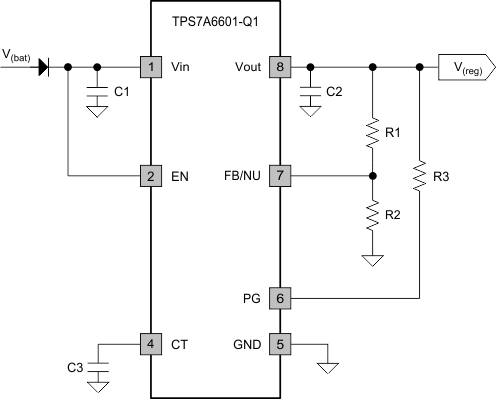
Adjustable Output Voltage (FB for TPS7A6601-Q1)

One can select an output voltage between 1.5 V and 5 V by using an external resistor divider. Calculate the output voltage using the following equation, where V(FB) = 1.223 V. The recommendation for R1 and R2 is that both be less than 100 kΩ.

Equation 2. TPS7A66-Q1 TPS7A69-Q1 eq2_vout_SLVSBL0.gif
TPS7A66-Q1 TPS7A69-Q1 Ext_Fdbk_Res_SLVSBL0.gifFigure 23. External Feedback Resistor Divider