ZHCSAO4F December 2012 – March 2018 UCC27611
PRODUCTION DATA.
7.3.1 VDD and Undervoltage Lockout
The UCC27611 device has internal Under Voltage LockOut (UVLO) protection feature on the VDD pin supply circuit blocks. Whenever the driver is in UVLO condition (that is when VDD voltage less than VDD(on) during power up, and when VDD voltage is less than VDD(off) during power down), this circuit holds all outputs LOW, regardless of the status of the inputs. The UVLO is typically 3.8 V, with 250-mV typical hysteresis. This hysteresis helps prevent chatter when low VDD supply voltages have noise from the power supply, and also when there are droops in the VDD bias voltage when the system commences switching and there is a sudden increase in IDD. The capability to operate at low-voltage levels such as below 5 V, along with best-in-class switching characteristics, is especially suited for driving emerging GaN wide bandgap power semiconductor devices.
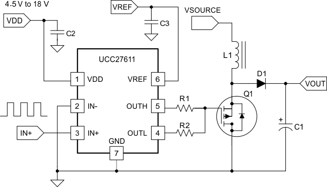
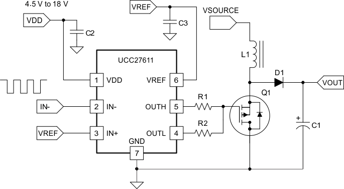
For example, at power up, the UCC27611 driver output remains LOW until the VDD voltage reaches the UVLO threshold. The magnitude of the OUT signal rises with VDD, until steady-state VDD is reached. In the noninverting operation (PWM signal applied to IN+ pin), see Figure 9, the output remains LOW until the UVLO threshold is reached, and then the output is in-phase with the input. In the inverting operation (PWM signal applied to IN– pin), see Figure 10, the output remains LOW until the UVLO threshold is reached, and then the output is out-phase with the input. In both cases, the unused input pin must be properly biased to enable the output.
NOTE
The output turns to high state only if IN+ pin is high and IN– pin is low after the UVLO threshold is reached.

