ZHCSBC4D May 2013 – May 2017 TAS5760MD
PRODUCTION DATA.
- 1 特性
- 2 应用
- 3 说明
- 4 修订历史记录
- 5 Device Comparison Table
- 6 Pin Configuration and Functions
-
7 Specifications
- 7.1 Absolute Maximum Ratings
- 7.2 ESD Ratings
- 7.3 Recommended Operating Conditions
- 7.4 Thermal Information
- 7.5 Digital I/O Pins
- 7.6 Master Clock
- 7.7 Serial Audio Port
- 7.8 Protection Circuitry
- 7.9 Speaker Amplifier in All Modes
- 7.10 Headphone Amplifier and Line Driver
- 7.11 I²C Control Port
- 7.12 Typical Idle, Mute, Shutdown, Operational Power Consumption
-
8 Detailed Description
- 8.1 Overview
- 8.2 Functional Block Diagram
- 8.3 Feature Description
- 8.4
Device Functional Modes
- 8.4.1
Hardware Control Mode
- 8.4.1.1 Speaker Amplifier Shut Down (SPK_SD Pin)
- 8.4.1.2 Serial Audio Port in Hardware Control Mode
- 8.4.1.3 Soft Clipper Control (SFT_CLIP Pin)
- 8.4.1.4 Speaker Amplifier Switching Frequency Select (FREQ/SDA Pin)
- 8.4.1.5 Parallel Bridge Tied Load Mode Select (PBTL/SCL Pin)
- 8.4.1.6 Speaker Amplifier Sleep Enable (SPK_SLEEP/ADR Pin)
- 8.4.1.7 Speaker Amplifier Gain Select (SPK_GAIN [1:0] Pins)
- 8.4.1.8 Considerations for Setting the Speaker Amplifier Gain Structure
- 8.4.2 Software Control Mode
- 8.4.1
Hardware Control Mode
- 8.5
Register Maps
- 8.5.1 Control Port Registers - Quick Reference
- 8.5.2
Control Port Registers - Detailed Description
- 8.5.2.1 Device Identification Register (0x00)
- 8.5.2.2 Power Control Register (0x01)
- 8.5.2.3 Digital Control Register (0x02)
- 8.5.2.4 Volume Control Configuration Register (0x03)
- 8.5.2.5 Left Channel Volume Control Register (0x04)
- 8.5.2.6 Right Channel Volume Control Register (0x05)
- 8.5.2.7 Analog Control Register (0x06)
- 8.5.2.8 Reserved Register (0x07)
- 8.5.2.9 Fault Configuration and Error Status Register (0x08)
- 8.5.2.10 Reserved Controls (9 / 0x09) - (15 / 0x0F)
- 8.5.2.11 Digital Clipper Control 2 Register (0x10)
- 8.5.2.12 Digital Clipper Control 1 Register (0x11)
-
9 Application and Implementation
- 9.1 Application Information
- 9.2
Typical Applications
- 9.2.1
Stereo BTL Using Software Control
- 9.2.1.1 Design Requirements
- 9.2.1.2
Detailed Design Procedure
- 9.2.1.2.1 Startup Procedures- Software Control Mode
- 9.2.1.2.2 Shutdown Procedures- Software Control Mode
- 9.2.1.2.3 Component Selection and Hardware Connections
- 9.2.1.2.4 Recommended Startup and Shutdown Procedures
- 9.2.1.2.5
Headphone and Line Driver Amplifier
- 9.2.1.2.5.1 Charge-Pump Flying Capacitor and DR_VSS Capacitor
- 9.2.1.2.5.2 Decoupling Capacitors
- 9.2.1.2.5.3 Gain-Setting Resistor Ranges
- 9.2.1.2.5.4 Using the Line Driver Amplifier in the TAS5760MD as a Second-Order Filter
- 9.2.1.2.5.5 External Undervoltage Detection
- 9.2.1.2.5.6 Input-Blocking Capacitors
- 9.2.1.2.6 Gain-Setting Resistors
- 9.2.1.3 Application Curve
- 9.2.2 Stereo BTL Using Hardware Control
- 9.2.3 Mono PBTL Using Software Control
- 9.2.4 Mono PBTL Using Hardware Control
- 9.2.1
Stereo BTL Using Software Control
- 10Power Supply Recommendations
- 11Layout
- 12器件和文档支持
- 13机械、封装和可订购信息
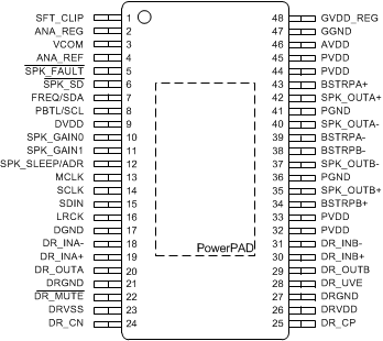
6 Pin Configuration and Functions
DCA Package
48 Pins TSSOP
Top View
