ZHCSBD2B September 2013 – January 2015 TPA3131D2 , TPA3132D2
PRODUCTION DATA.
- 1 特性
- 2 应用
- 3 说明
- 4 修订历史记录
- 5 Pin Configuration and Functions
- 6 Specifications
-
7 Detailed Description
- 7.1 Overview
- 7.2 Functional Block Diagram
- 7.3
Feature Description
- 7.3.1 Gain Setting and Master and Slave
- 7.3.2 Input Impedance
- 7.3.3 Start-up/Shutdown Operation
- 7.3.4 PLIMIT Operation
- 7.3.5 GVDD Supply
- 7.3.6 BSPx and BSNx Capacitors
- 7.3.7 Differential Inputs
- 7.3.8 Device Protection System
- 7.3.9 DC Detect Protection
- 7.3.10 Short-Circuit Protection and Automatic Recovery Feature
- 7.3.11 Thermal Protection
- 7.3.12 Efficiency: LC Filter Required with the Traditional Class-D Modulation Scheme
- 7.3.13 Ferrite Bead Filter Considerations
- 7.3.14 When to Use an Output Filter for EMI Suppression
- 7.3.15 AM Avoidance EMI Reduction
- 7.4 Device Functional Modes
- 8 Applications and Implementation
- 9 Power Supply Recommendations
- 10Layout
- 11器件和文档支持
- 12机械、封装和可订购信息
10 Layout
10.1 Layout Guidelines
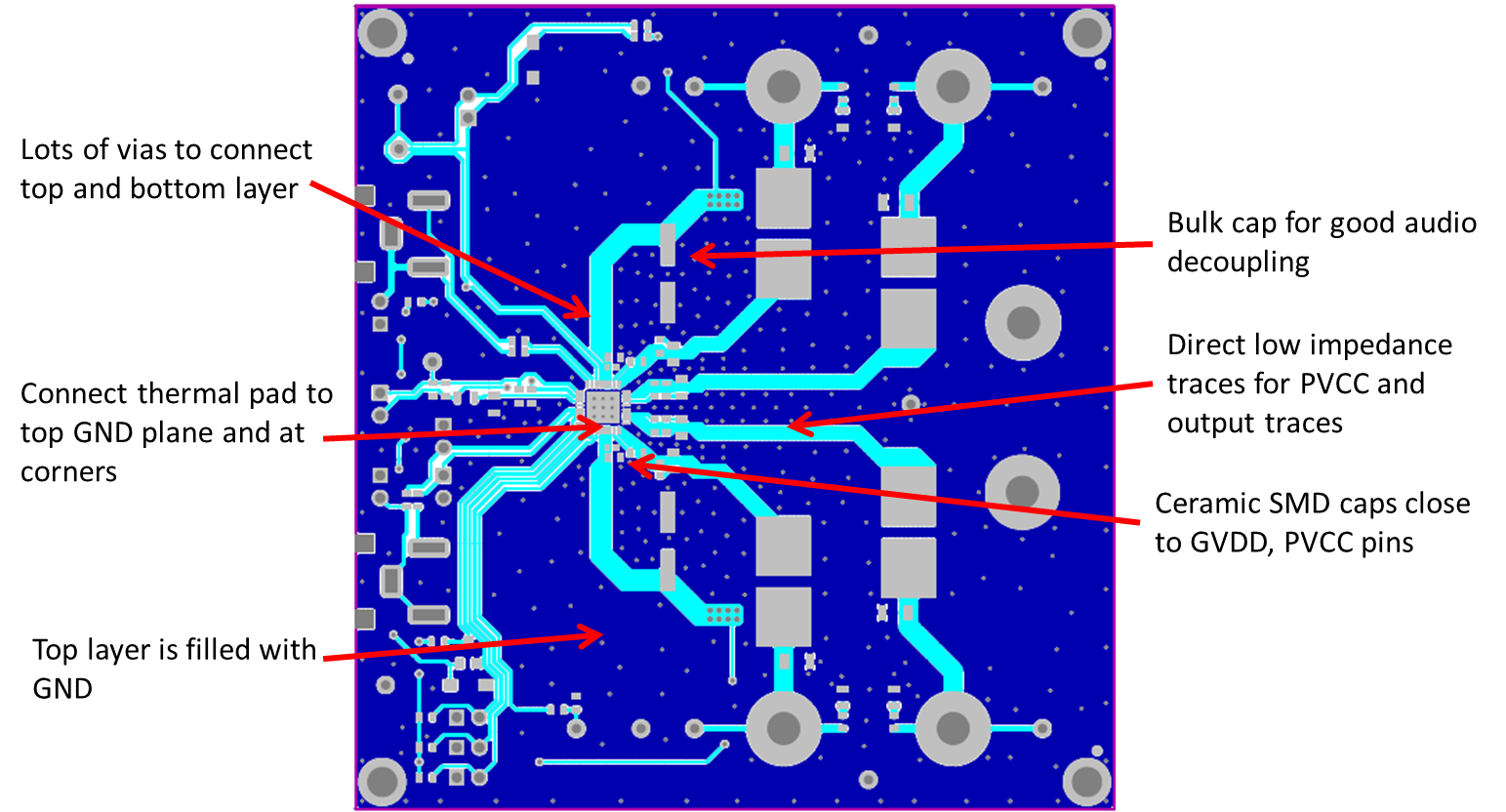
The TPA313xD2 can be used with a small, inexpensive ferrite bead output filter for most applications. However, since the class-D switching edges are fast, it is necessary to take care when planning the layout of the printed circuit board. The following suggestions will help to meet EMC requirements.
- Decoupling capacitors — The high-frequency decoupling capacitors should be placed as close to the PVCC and AVCC terminals as possible. Large (100 μF or greater) bulk power supply decoupling capacitors should be placed near the TPA313xD2 on the PVCC supplies. Local, high-frequency bypass capacitors should be placed as close to the PVCC pins as possible. These caps can be connected to the IC GND pad directly for an excellent ground connection. Consider adding a small, good quality low ESR ceramic capacitor between 220 pF and 1 nF and a larger mid-frequency cap of value between 100 nF and 1 µF also of good quality to the PVCC connections at each end of the chip.
- Keep the current loop from each of the outputs through the ferrite bead and the small filter cap and back to GND as small and tight as possible. The size of this current loop determines its effectiveness as an antenna.
- Grounding — The PVCC decoupling capacitors should connect to GND. All ground should be connected at the IC GND, which should be used as a central ground connection or star ground for the TPA313xD2.
- Output filter — The ferrite EMI filter (see Figure 27) should be placed as close to the output terminals as possible for the best EMI performance. The LC filter should be placed close to the outputs. The capacitors used in both the ferrite and LC filters should be grounded.
For an example layout, see the TPA313xD2 Evaluation Module (TPA313xD2EVM) User Manual. Both the EVM user manual and the thermal pad application report are available on the TI Web site at http://www.ti.com.
10.2 Layout Example
 Figure 32. Layout Example Top
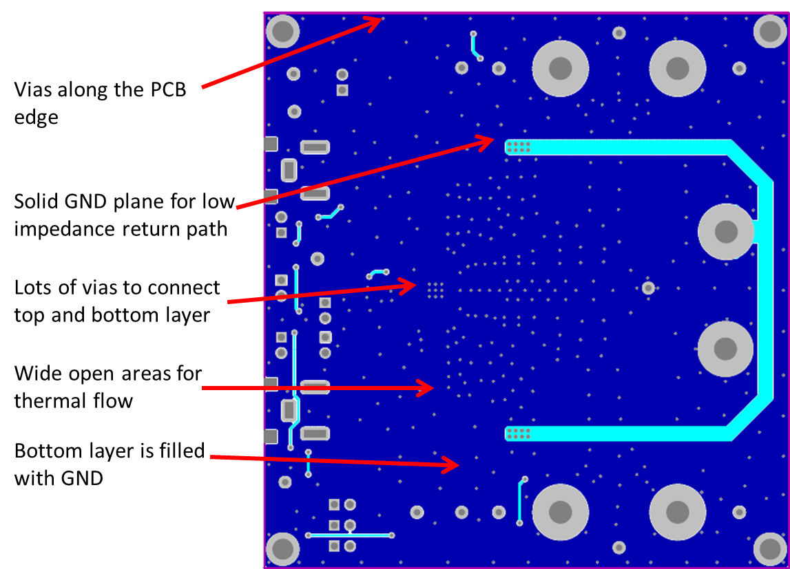
 Figure 33. Layout Example Bottom
10.3 Thermal Design
Main thermal path for cooling the device is from the bottom side PowerPAD through multiple via connections in the PCB to the bottom side ground plane. The high power efficiency allows TPA3131D2 to be operated continuously at rated output power into both 4-Ω and 8-Ω load, and TPA3132D2 into 8-Ω load using a PCB layout similar to what is used in the TPA3131D2/32D2 EVMs. The rated output power of TPA3132D2 into 4-Ω load will be available only for a limited duration of time when using a PCB layout similar to the EVM layout. Sustained power output into 4 Ω needs to be limited to prevent excess heating of the device. TPA3132D2 will be able to output full output power for a limited duration of time. The duration depends on the actual PCB layout. For the TPA3132D2 EVM layout the TPA3132D2 full output power with 4-Ω load can be illustrated with a burst test at room temp (25°C):
Table 7. TPA3132D2 EVM Burst Output Power
| BURST RATIO | FULL POWER 1kHz | REDUCED POWER 1kHz (1/8 of full power) |
MAXIMUM DEVICE TEMPERATURE | PCB TEMPERATURE (Bottom Side, Under Device) |
|---|---|---|---|---|
| 1:3 | 1 Cycle 44 W / 4 Ω | 2 Cycles 5.25 W / 4 Ω | 116°C | 85°C |
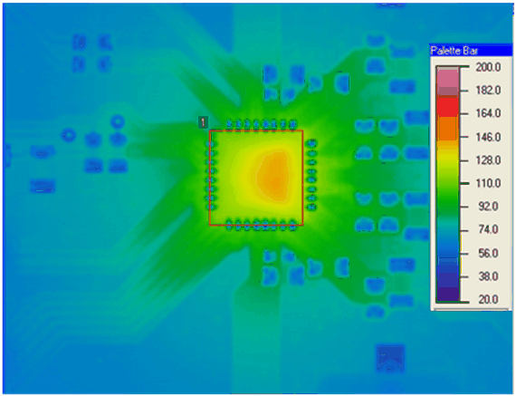
| 2:5 | 2 Cycles 44 W / 4 Ω | 3 Cycles 5.25 W / 4 Ω | 143°C | 102°C |
It is not recommended to operate the device with a maximum temperature above 150°C.
 Figure 34. TPA3132D2 EVM Temperature with 2:5 (42W/5.25W/4Ω) Burst Power
It is advised to use the PLIMT function to avoid thermal shutdown in system designs not using signal processing to limit the average output power. Such systems can accidentally exceed the thermal limits of the amplifier and a OTE shutdown will occur.