ZHCSBG2B May 2013 – February 2019 ADS8860
PRODUCTION DATA.
- 1 特性
- 2 应用
- 3 说明
- 4 修订历史记录
- 5 Device Comparison Table
- 6 Pin Configuration and Functions
- 7 Specifications
- 8 Parameter Measurement Information
- 9 Detailed Description
- 10Application and Implementation
- 11Power Supply Recommendations
- 12Layout
- 13器件和文档支持
- 14机械、封装和可订购信息
9.4.1.1 3-Wire CS Mode Without a Busy Indicator
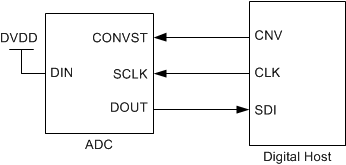
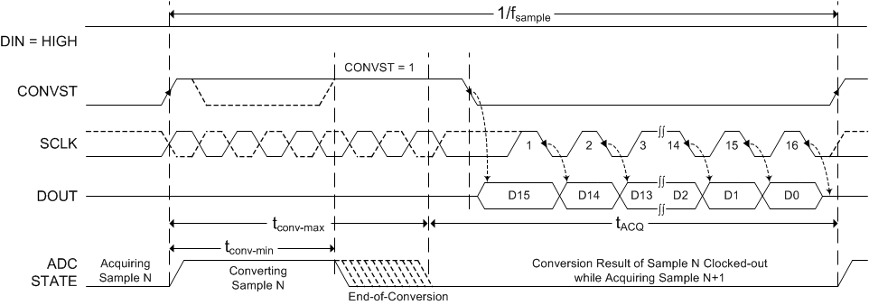
This interface option is most useful when a single ADC is connected to an SPI-compatible digital host. In this interface option, DIN can be connected to DVDD and CONVST functions as CS (as shown in Figure 48). As shown in Figure 49, a CONVST rising edge forces DOUT to 3-state, samples the input signal, and causes the device to enter a conversion phase. Conversion is done with the internal clock and continues regardless of the state of CONVST. As a result, CONVST (functioning as CS) can be pulled low after the start of the conversion to select other devices on the board. However, CONVST must return high before the minimum conversion time (tconv-min) elapses and is held high until the maximum possible conversion time (tconv-max) elapses. A high level on CONVST at the end of the conversion ensures the device does not generate a busy indicator.
 Figure 48. Connection Diagram: 3-Wire CS Mode Without a Busy Indicator (DIN = 1)
  Figure 49. Interface Timing Diagram: 3-Wire CS Mode Without a Busy Indicator (DIN = 1)
 When conversion is complete, the device enters an acquisition phase and powers down. CONVST (functioning as CS) can be brought low after the maximum conversion time (tconv-max) elapses. On the CONVST falling edge, DOUT comes out of 3-state and the device outputs the MSB of the data. The lower data bits are output on subsequent SCLK falling edges. Fast sampling rates require high frequency SCLK and data must be read at SCLK falling edges. For slow sampling rates and SCLK frequency ≤ 36 MHz, data can be read at either SCLK falling or rising edges. Note that with any SCLK frequency, reading data at SCLK falling edge requires the digital host to clock in the data during the th_CK_DO-min time frame. DOUT goes to 3-state after the 16th SCLK falling edge or when CONVST goes high, whichever occurs first.