ZHCSBS1A November 2013 – August 2015 HD3SS6126
PRODUCTION DATA.
8 Application and Implementation
NOTE
Information in the following applications sections is not part of the TI component specification, and TI does not warrant its accuracy or completeness. TI’s customers are responsible for determining suitability of components for their purposes. Customers should validate and test their design implementation to confirm system functionality.
8.1 Application Information
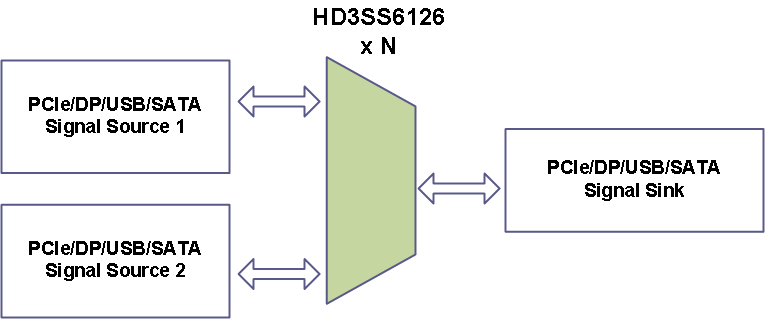
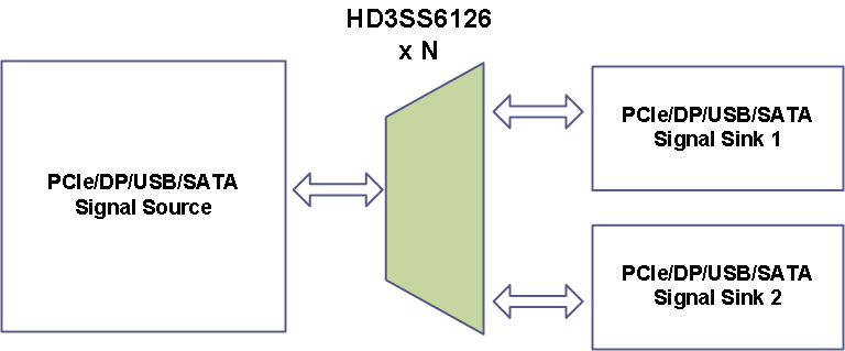
A typical application for the HD3SS6126 is a USB 3.0 KVM switch, where one of two USB hosts system can be selected for an USB device. These guidelines are also suitable for PCIe(Gen1,Gen2), SATA, XAUI and DP, since the HD3SS6126 device is fully compatible with these protocols.
8.2 Typical Application
 Figure 6. Two Signal Sources to One Destination
 Figure 7. One Signal Sources to Two Destination
8.2.1 Design Requirements
Power supply requirements:
- VDD from 3 V to 3.6 V
Control pins requirements
- VIH from 2 V to VDD
- VIL from –0.1 V to 0.8 V
Differential pairs requirements:
- VI/O_Diff from 0 V to 1.8 Vp-p
- VI/O_CM from 0 V to 2 V
TA Operating free-air temperature from 0°C to 70°C
8.2.2 Detailed Design Procedure
8.2.2.1 Power Supply
The first step is to design the power supply and determine the VCC stability and minimum current required (see Power Supply Recommendations).
8.2.2.2 Differential Pairs
All of the interfaces the HD3SS6126 device supports require AC coupling between the transmitter and receiver. TI recommends using 0402-sized capacitors to provide AC coupling, but 0603-sized capacitors are also acceptable. Both 0805-sized capacitors and C-packs should be avoided. Best practice is to place AC-coupling capacitors symmetrically. A capacitor value of 0.1uF is best and the value should be matched for the +/-signal pair. The placement should be along the TX pairs on the system board, which are usually routed on the top layer of the board.
All differential pairs must have a matched impedance according to the implemented protocol: 100-Ω differential (±10%) for PCIe and 90-Ω differential (±15%) for USB 2.0 and USB 3.0.
The control logic can be implemented by use of an external control processor or by using a simple selector switch. TI recommends using 5-kΩ pullup and pulldown resistors on the control signals, if they are included. The control logic must not violate the input voltage parameters outlined in the Recommended Operating Conditions table.
8.2.3 Application Curves
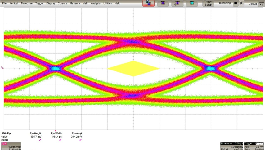
 Figure 8. USB 3.0 TX Eye Pattern Test With 3-Inch 5-mil Differential PCB Trace Without HD3SS6126
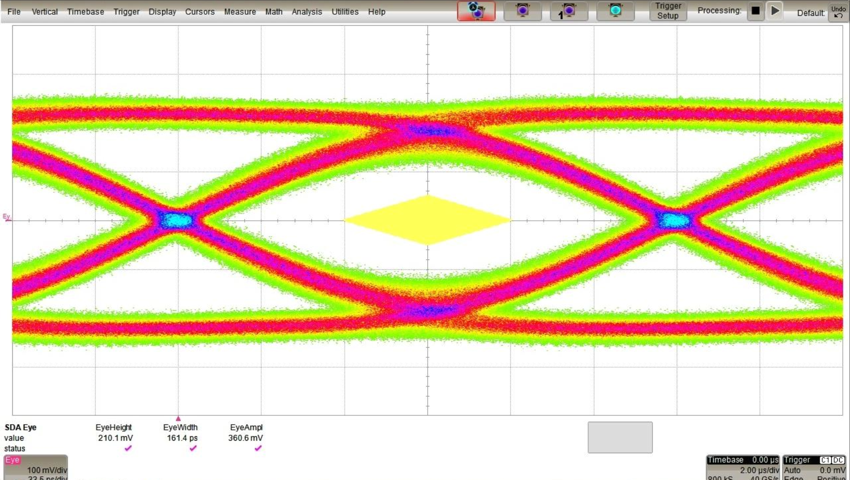
 Figure 9. USB 3.0 TX Eye Pattern Test With 3-Inch 5-mil Differential PCB Trace With HD3SS6126