ZHCSC40E February   2014  – May 2018 TPS92630-Q1

PRODUCTION DATA.  

  1. 特性
  2. 应用
  3. 说明
    1.     Device Images
      1.      典型应用原理图
  4. 修订历史记录
  5. 说明 (续)
  6. Pin Configuration and Functions
    1.     Pin Functions
  7. Specifications
    1. 7.1 Absolute Maximum Ratings
    2. 7.2 ESD Ratings
    3. 7.3 Recommended Operating Conditions
    4. 7.4 Thermal Information
    5. 7.5 Electrical Characteristics
    6. 7.6 Timing Requirements
    7. 7.7 Typical Characteristics
  8. Parameter Measurement Information
  9. Detailed Description
    1. 9.1 Overview
    2. 9.2 Functional Block Diagram
    3. 9.3 Feature Description
      1. 9.3.1 Constant LED-Current Setting
      2. 9.3.2 PWM Control
      3. 9.3.3 FAULT Diagnostics
      4. 9.3.4 Short-Circuit Detection
      5. 9.3.5 Open-Load Detection
      6. 9.3.6 Thermal Foldback
    4. 9.4 Device Functional Modes
      1. 9.4.1 Thermal Information
      2. 9.4.2 Operation With V(VIN) < 5 V (Minimum V(VIN))
      3. 9.4.3 Operation With 5 V < V(VIN) < 9 V (Lower-Than-Normal Automotive Battery Voltage)
  10. 10Applications and Implementation
    1. 10.1 Application Information
    2. 10.2 Typical Applications
      1. 10.2.1 Stoplight and Taillight Application With PWM Generator
        1. 10.2.1.1 Design Requirements
        2. 10.2.1.2 Detailed Design Procedure
          1. 10.2.1.2.1 Step-by-Step Design Procedure
            1. 10.2.1.2.1.1 R(REF)
            2. 10.2.1.2.1.2 Duty Cycle
            3. 10.2.1.2.1.3 Input and Output Capacitors
        3. 10.2.1.3 PWM Dimming Application Curve
      2. 10.2.2 Simple Stop-Light and Taillight Application
        1. 10.2.2.1 Design Requirements
        2. 10.2.2.2 Detailed Design Procedure
          1. 10.2.2.2.1 Step-by-Step Design Procedure
            1. 10.2.2.2.1.1 R(REF)
            2. 10.2.2.2.1.2 R(Stop)
            3. 10.2.2.2.1.3 Input and Output Capacitors
      3. 10.2.3 Parallel Connection
        1. 10.2.3.1 Design Requirements
        2. 10.2.3.2 Detailed Design Procedure
          1. 10.2.3.2.1 Step-by-Step Design Procedure
            1. 10.2.3.2.1.1 R(REF)
            2. 10.2.3.2.1.2 Input and Output Capacitors
      4. 10.2.4 Alternate Parallel Connection
        1. 10.2.4.1 Design Requirements
        2. 10.2.4.2 Detailed Design Procedure
          1. 10.2.4.2.1 Step-by-Step Design Procedure
            1. 10.2.4.2.1.1 R(REF)
            2. 10.2.4.2.1.2 Input and Output Capacitors
      5. 10.2.5 High-Side PWM Dimming
        1. 10.2.5.1 Design Requirements
        2. 10.2.5.2 Detailed Design Procedure
          1. 10.2.5.2.1 Step-by-Step Design Procedure
            1. 10.2.5.2.1.1 Ratio of Resistors, R1 / R2
            2. 10.2.5.2.1.2 R1 and R2 Selection
            3. 10.2.5.2.1.3 Input and Output Capacitors
  11. 11Power Supply Recommendations
  12. 12Layout
    1. 12.1 Layout Guidelines
    2. 12.2 Layout Example
  13. 13器件和文档支持
    1. 13.1 文档支持
      1. 13.1.1 相关文档
    2. 13.2 接收文档更新通知
    3. 13.3 社区资源
    4. 13.4 商标
    5. 13.5 静电放电警告
    6. 13.6 术语表
  14. 14机械、封装和可订购信息

Typical Characteristics

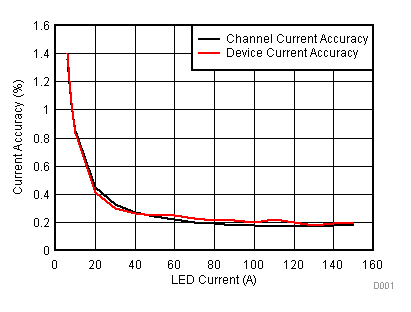
TPS92630-Q1 D001_SLVSC76.gif
TA = 25ºC V(VIN) = 14 V Three LEDs
Figure 1. Current Accuracy vs Current Setting
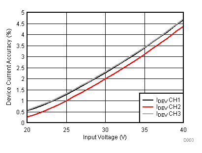
TPS92630-Q1 D003_SLVSC76.gif
V(VIN) = 20 V I(setting) = 150 mA
Figure 3. Device Current Accuracy vs Input Voltage
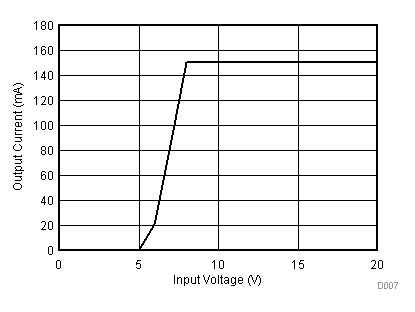
TPS92630-Q1 D007_SLVSC76.gif
3 white LEDs LEDs in series I(setting) = 150 mA
Figure 5. Output Current vs Input Voltage
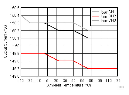
TPS92630-Q1 D009_SLVSC76.gif
I(setting)= 150 mA V(VIN) = 14 V
Figure 7. Output Current vs Ambient Temperature
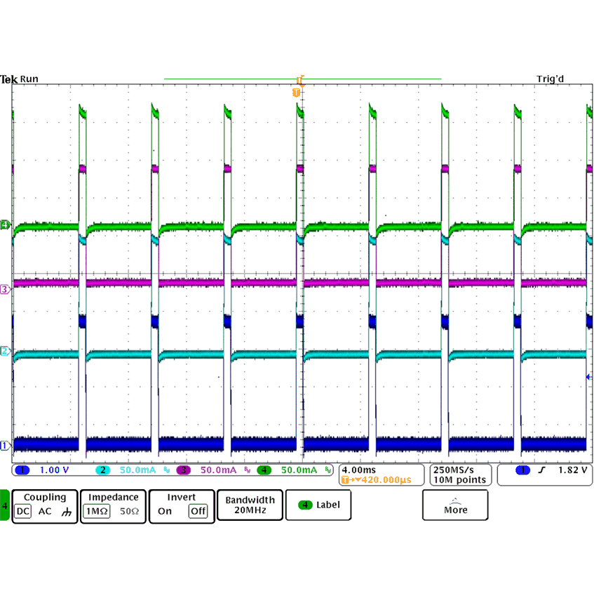
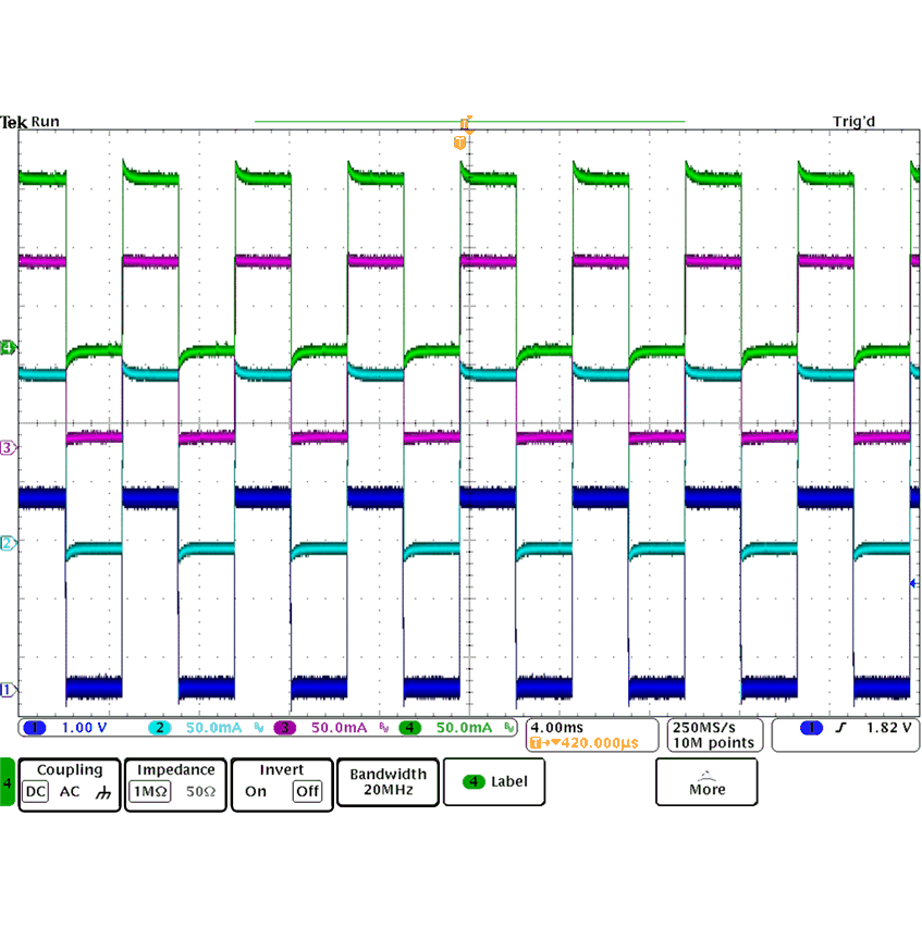
TPS92630-Q1 PWM_200Hz_10Percent_SLVSC76.gif
Ch. 1 = PWM input Ch. 2 = IOUT1 Ch. 3 = IOUT2
Ch. 4 = IOUT3 f(PWM) = 200 Hz Duty cycle = 10%
Figure 9. PWM Dimming
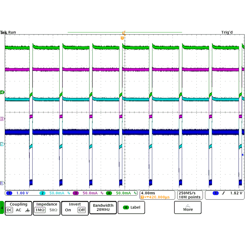
TPS92630-Q1 PWM_200Hz_90Percent_SLVSC76.gif
Ch. 1 = PWM input Ch. 2 = IOUT1 Ch. 3 = IOUT2
Ch. 4 = IOUT3 f(PWM) = 200 Hz Duty cycle = 90%
Figure 11. PWM Dimming
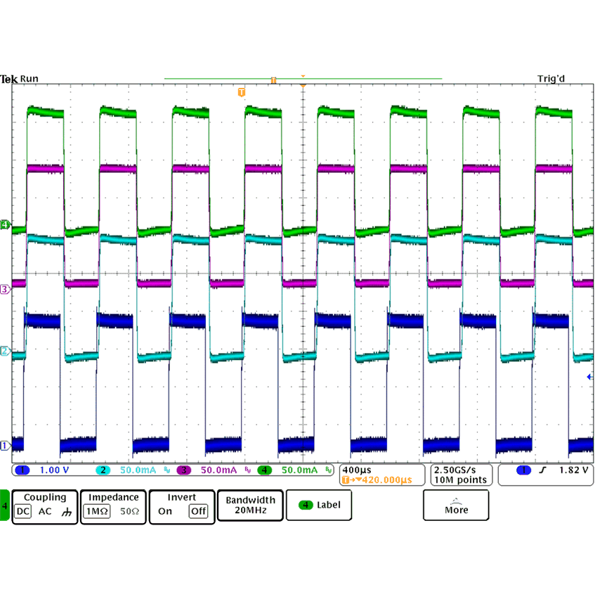
TPS92630-Q1 PWM_2kHz_50Percent_SLVSC76.gif
Ch. 1 = PWM input Ch. 2 = IOUT1 Ch. 3 = IOUT2
Ch. 4 = IOUT3 f(PWM) = 2000 Hz Duty cycle = 50%
Figure 13. PWM Dimming
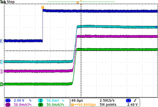
TPS92630-Q1 Power_Up_Waveform_SLVSC76.gif
I(setting) = 60 mA
Figure 15. Fast Power-Up Waveform
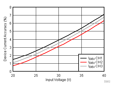
TPS92630-Q1 D002_SLVSC76.gif
V(VIN) = 20 V I(setting) = 30 mA
Figure 2. Device Current Accuracy vs Input Voltage
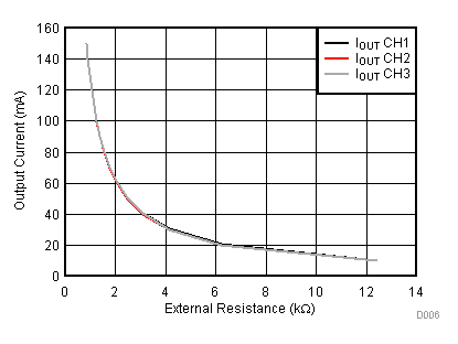
TPS92630-Q1 D006_SLVSC76.gif
A
Figure 4. Output Current vs External Resistance
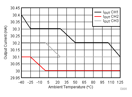
TPS92630-Q1 D008_SLVSC76.gif
I(setting) = 30 mA V(VIN) = 14 V
Figure 6. Output Current vs Ambient Temperature
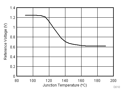
TPS92630-Q1 D010_SLVSC76.gif
A
Figure 8. Reference Voltage vs Junction Temperature With Thermal Foldback
TPS92630-Q1 PWM_200Hz_50Percent_SLVSC76.gif
Ch. 1 = PWM input Ch. 2 = IOUT1 Ch. 3 = IOUT2
Ch. 4 = IOUT3 f(PWM) = 200 Hz Duty cycle = 50%
Figure 10. PWM Dimming
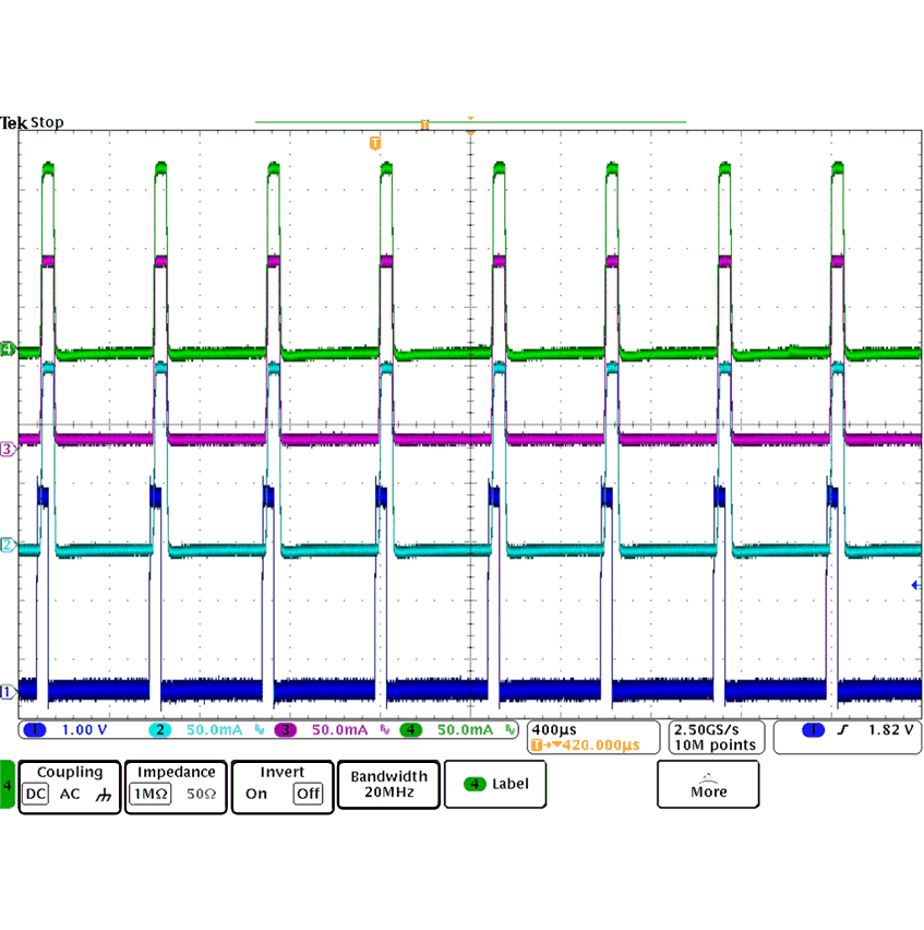
TPS92630-Q1 PWM_2kHz_10Percent_SLVSC76.gif
Ch. 1 = PWM input Ch. 2 = IOUT1 Ch. 3 = IOUT2
Ch. 4 = IOUT3 f(PWM) = 2000 Hz Duty cycle = 10%
Figure 12. PWM Dimming
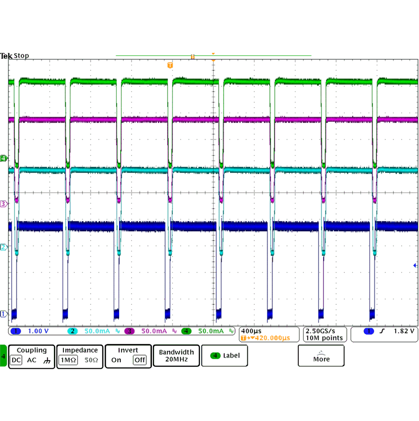
TPS92630-Q1 PWM_2kHz_90Percent_SLVSC76.gif
Ch. 1 = PWM input Ch. 2 = IOUT1 Ch. 3 = IOUT2
Ch. 4 = IOUT3 f(PWM) = 2000 Hz Duty cycle = 90%
Figure 14. PWM Dimming
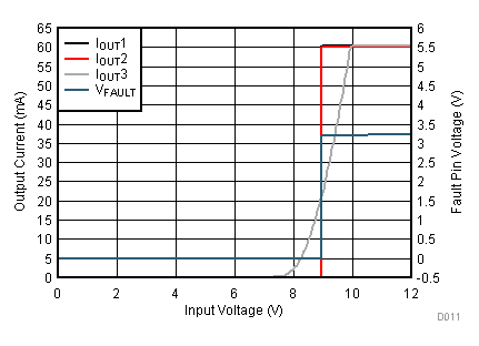
TPS92630-Q1 D011_SLVSC76.gif
V(VIN) = V(EN) V(VIN) = 0 V to 12 V I(setting) = 60 mA
3 white LEDs dV/dt = 0.5 V/min
Figure 16. Slow Power-Up Waveform