ZHCSC62D March 2014 – December 2017 UCC28630 , UCC28631 , UCC28632 , UCC28633 , UCC28634
PRODUCTION DATA.
- 1 特性
- 2 应用
- 3 说明
- 4 修订历史记录
- 5 Device Comparison Table
- 6 Pin Configuration and Functions
- 7 Specifications
-
8 Detailed Description
- 8.1 Overview
- 8.2 Functional Block Diagram
- 8.3
Feature Description
- 8.3.1 High-Voltage Current Source Start-Up Operation
- 8.3.2 AC Input UVLO / Brownout Protection
- 8.3.3 Active X-Capacitor Discharge (UCC28630 and UCC28633 only)
- 8.3.4 Magnetic Input and Output Voltage Sensing
- 8.3.5 Fixed-Point Magnetic Sense Sampling Error Sources
- 8.3.6 Magnetic Sense Resistor Network Calculations
- 8.3.7 Magnetic Sensing: Power Stage Design Constraints
- 8.3.8 Magnetic Sense Voltage Control Loop
- 8.3.9 Peak Current Mode Control
- 8.3.10 IPEAK Adjust vs. Line
- 8.3.11 Primary-Side Constant-Current Limit (CC Mode)
- 8.3.12 Primary-Side Overload Timer (UCC28630 only)
- 8.3.13 Overload Timer Adjustment (UCC28630 only)
- 8.3.14 CC-Mode IOUT(lim) Adjustment
- 8.3.15 Fault Protections
- 8.3.16 Pin-Fault Detection and Protection
- 8.3.17 Over-Temperature Protection
- 8.3.18 External Fault Input
- 8.3.19 External SD Pin Wake Input (except UCC28633)
- 8.3.20 External Wake Input at VSENSE Pin (UCC28633 Only)
- 8.3.21 Mode Control and Switching Frequency Modulation
- 8.3.22 Frequency Dither For EMI (except UCC28632)
- 8.4 Device Functional Modes
-
9 Applications and Implementation
- 9.1 Application Information
- 9.2
Typical Application
- 9.2.1 Notebook Adapter, 19.5 V, 65 W
- 9.2.2 UCC28630 Application Schematic
- 9.2.3 Design Requirements
- 9.2.4
Detailed Design Procedure
- 9.2.4.1 Custom Design With WEBENCH® Tools
- 9.2.4.2 Input Bulk Capacitance and Minimum Bulk Voltage
- 9.2.4.3 Transformer Turn Ratio
- 9.2.4.4 Transformer Magnetizing Inductance
- 9.2.4.5 Current Sense Resistor RCS
- 9.2.4.6 Transformer Constraint Verification
- 9.2.4.7 Transformer Selection and Design
- 9.2.4.8 Slope Compensation Verification
- 9.2.4.9 Power MOSFET and Output Rectifier Selection
- 9.2.4.10 Output Capacitor Selection
- 9.2.4.11 Calculation of CC Mode Limit Point
- 9.2.4.12 VDD Capacitor Selection
- 9.2.4.13 Magnetic Sense Resistor Network Selection
- 9.2.4.14 Output LED Pre-Load Resistor Calculation
- 9.2.5 External Wake Pulse Calculation at VSENSE Pin (UCC28633 Only)
- 9.2.6 Energy Star Average Efficiency and Standby Power
- 9.2.7 Application Performance Plots
- 9.3 Dos and Don'ts
- 10Power Supply Recommendations
- 11Layout
- 12器件和文档支持
- 13机械、封装和可订购信息
8.3.1 High-Voltage Current Source Start-Up Operation
The controller includes a switched, high-voltage, current source on the HV pin to allow fast start-up, and eliminates the static power dissipation in a conventional resistive start-up approach. This feature reduces standby power consumption.
The HV pin has three major functions:
- Supply the device start-up current
- Supply the device bias power during latched fault mode
- AC sense input for X-capacitor discharge detect (UCC28630 and UCC28633 only)
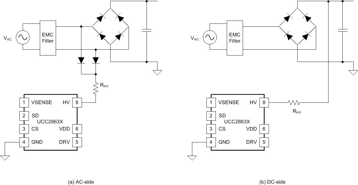
The UCC28630 and UCC28633 input supply to the HV start-up pin must be connected to the AC side of the bridge rectifier as shown in Figure 15, in order to support X-capacitor discharge. More details are given in Active X-Capacitor Discharge (UCC28630 and UCC28633 only), below. Connection to the AC side of the bridge also allows faster detection of AC mains removal under latched fault conditions, allowing prompt reset of latched faults for fast restart.
In the UCC28631, UCC28632 and UCC28634, the HV pin can connect to either the AC or DC side of the bridge. The addition of the 200-kΩ external HV resistance (required for X-capacitor discharge sensing) limits the available charging current for the external bias supply input capacitor. However, for typical values of between 22 µF and 33 µF of input capacitance, start-up bias times of less than 1.5 s are achievable at 90 VAC. Start-up time can be estimated using Equation 1.
For 90 VAC, if CVDD = 22 µF and worst case VDD(start_max) = 16.5 V, then tSTART is 1.002 s.
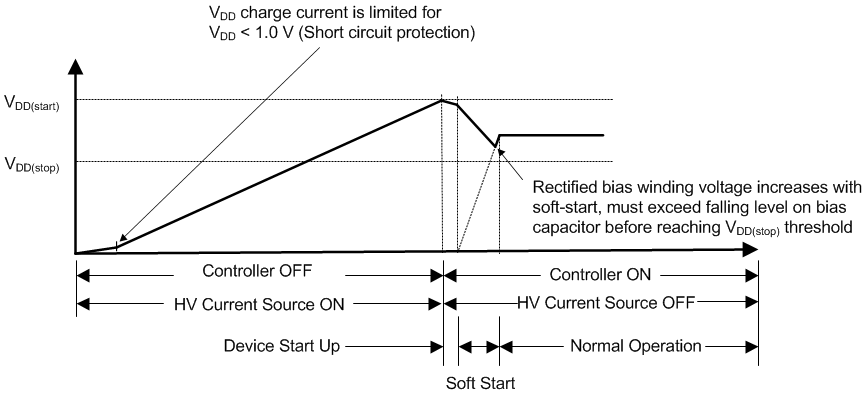
Figure 16 illustrates the start-up behavior of the controller. The HV current source has built-in short-circuit protection that limits the initial charge current out of the bias voltage pin until the bias voltage reaches VDD(sc). This limits the power dissipated in the HV current source in the event of a short circuit on the VDD pin. Thereafter, the HV current source switches to full available current. The controller remains in a low-power, start-up mode until the bias voltage reaches VDD(start), after which the HV current source is turned off and the controller initiates a start-up sequence.
The bias voltage decays during the start-up sequence at a rate dependent on the size of the energy storage capacitor connected to the VDD pin. The VDD storage capacitor must be sized appropriately to ensure adequate energy storage to supply both the controller bias power and MOSFET drive power during start-up, until the VDD rail can be supplied through the transformer bias winding. If the bias voltage falls below VDD(stop) (due to bias winding fault or an inadequate VDD storage capacitance), the controller stops switching, and transitions into low-power mode for a time delay of tRESET(long), or until the bias voltage falls to the VDD(reset) level, whichever is shorter. See VDD Capacitor Selection for required VDD capacitor sizing. Once the time delay elapses, the bias voltage rapidly discharges to the VDD(reset) level, followed by turn-on of the internal HV current source, and a normal restart attempt follows.
 Figure 16. Normal Start-Up Sequence,
 (assuming VAC > UV start threshold)


 for AC connection and VIN(avg) = VRMS x √2 for DC connection