ZHCSC62D March 2014 – December 2017 UCC28630 , UCC28631 , UCC28632 , UCC28633 , UCC28634
PRODUCTION DATA.
- 1 特性
- 2 应用
- 3 说明
- 4 修订历史记录
- 5 Device Comparison Table
- 6 Pin Configuration and Functions
- 7 Specifications
-
8 Detailed Description
- 8.1 Overview
- 8.2 Functional Block Diagram
- 8.3
Feature Description
- 8.3.1 High-Voltage Current Source Start-Up Operation
- 8.3.2 AC Input UVLO / Brownout Protection
- 8.3.3 Active X-Capacitor Discharge (UCC28630 and UCC28633 only)
- 8.3.4 Magnetic Input and Output Voltage Sensing
- 8.3.5 Fixed-Point Magnetic Sense Sampling Error Sources
- 8.3.6 Magnetic Sense Resistor Network Calculations
- 8.3.7 Magnetic Sensing: Power Stage Design Constraints
- 8.3.8 Magnetic Sense Voltage Control Loop
- 8.3.9 Peak Current Mode Control
- 8.3.10 IPEAK Adjust vs. Line
- 8.3.11 Primary-Side Constant-Current Limit (CC Mode)
- 8.3.12 Primary-Side Overload Timer (UCC28630 only)
- 8.3.13 Overload Timer Adjustment (UCC28630 only)
- 8.3.14 CC-Mode IOUT(lim) Adjustment
- 8.3.15 Fault Protections
- 8.3.16 Pin-Fault Detection and Protection
- 8.3.17 Over-Temperature Protection
- 8.3.18 External Fault Input
- 8.3.19 External SD Pin Wake Input (except UCC28633)
- 8.3.20 External Wake Input at VSENSE Pin (UCC28633 Only)
- 8.3.21 Mode Control and Switching Frequency Modulation
- 8.3.22 Frequency Dither For EMI (except UCC28632)
- 8.4 Device Functional Modes
-
9 Applications and Implementation
- 9.1 Application Information
- 9.2
Typical Application
- 9.2.1 Notebook Adapter, 19.5 V, 65 W
- 9.2.2 UCC28630 Application Schematic
- 9.2.3 Design Requirements
- 9.2.4
Detailed Design Procedure
- 9.2.4.1 Custom Design With WEBENCH® Tools
- 9.2.4.2 Input Bulk Capacitance and Minimum Bulk Voltage
- 9.2.4.3 Transformer Turn Ratio
- 9.2.4.4 Transformer Magnetizing Inductance
- 9.2.4.5 Current Sense Resistor RCS
- 9.2.4.6 Transformer Constraint Verification
- 9.2.4.7 Transformer Selection and Design
- 9.2.4.8 Slope Compensation Verification
- 9.2.4.9 Power MOSFET and Output Rectifier Selection
- 9.2.4.10 Output Capacitor Selection
- 9.2.4.11 Calculation of CC Mode Limit Point
- 9.2.4.12 VDD Capacitor Selection
- 9.2.4.13 Magnetic Sense Resistor Network Selection
- 9.2.4.14 Output LED Pre-Load Resistor Calculation
- 9.2.5 External Wake Pulse Calculation at VSENSE Pin (UCC28633 Only)
- 9.2.6 Energy Star Average Efficiency and Standby Power
- 9.2.7 Application Performance Plots
- 9.3 Dos and Don'ts
- 10Power Supply Recommendations
- 11Layout
- 12器件和文档支持
- 13机械、封装和可订购信息
8.3.3 Active X-Capacitor Discharge (UCC28630 and UCC28633 only)
Safety standards such as EN60950 require that any X-capacitors in EMC filters on the AC side of the bridge rectifier quickly discharge to a safe level when AC is disconnected. This discharge requirement ensures that any high-voltage level present at the pins of the AC plug does not present an electric shock hazard. The standards require that the voltage across the X-capacitor decay with a maximum time constant of 1 second. Typically, this requirement is achieved by including a resistive discharge element in parallel with the X-capacitor. However, this resistance causes a continuous power dissipation that impacts the standby power performance. The power dissipation in the discharge resistors depends on the X-capacitor value. Assuming that the discharge resistor meets the 1-second time-constant requirement, (in other words, the R-C product is 1 second) the dissipation is described in Equation 2.

Thus at 230 VAC, the discharge resistor causes 5.3-mW dissipation for every 100 nF of X-capacitance – for a typical 470-nF X-capacitor value, that causes 25 mW to be lost in the discharge resistors.
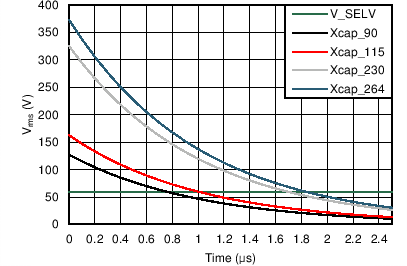
The safety standard does not mandate that the X-capacitor is fully discharged to zero within one second. It simply requires the discharge rate to exhibit a 1-s time constant. Figure 18shows the discharge characteristic (for a 1-s discharge time constant) versus time, for disconnection at the peak of 90 VAC, 115 VAC, 230 VAC and 264 VAC. For AC inputs above 115 VAC, with 1-s discharge time constant, the voltage does not drop below the Safety-Extra-Low-Voltage (SELV) 60-V level until 1 s or longer. In fact, at 264 VAC, 1.83 seconds elapse before reaching 60 V.
 Figure 18. X-Capacitor Discharge with 1-s Time Constant, for Various Voltages