ZHCSC62D March 2014 – December 2017 UCC28630 , UCC28631 , UCC28632 , UCC28633 , UCC28634
PRODUCTION DATA.
- 1 特性
- 2 应用
- 3 说明
- 4 修订历史记录
- 5 Device Comparison Table
- 6 Pin Configuration and Functions
- 7 Specifications
-
8 Detailed Description
- 8.1 Overview
- 8.2 Functional Block Diagram
- 8.3
Feature Description
- 8.3.1 High-Voltage Current Source Start-Up Operation
- 8.3.2 AC Input UVLO / Brownout Protection
- 8.3.3 Active X-Capacitor Discharge (UCC28630 and UCC28633 only)
- 8.3.4 Magnetic Input and Output Voltage Sensing
- 8.3.5 Fixed-Point Magnetic Sense Sampling Error Sources
- 8.3.6 Magnetic Sense Resistor Network Calculations
- 8.3.7 Magnetic Sensing: Power Stage Design Constraints
- 8.3.8 Magnetic Sense Voltage Control Loop
- 8.3.9 Peak Current Mode Control
- 8.3.10 IPEAK Adjust vs. Line
- 8.3.11 Primary-Side Constant-Current Limit (CC Mode)
- 8.3.12 Primary-Side Overload Timer (UCC28630 only)
- 8.3.13 Overload Timer Adjustment (UCC28630 only)
- 8.3.14 CC-Mode IOUT(lim) Adjustment
- 8.3.15 Fault Protections
- 8.3.16 Pin-Fault Detection and Protection
- 8.3.17 Over-Temperature Protection
- 8.3.18 External Fault Input
- 8.3.19 External SD Pin Wake Input (except UCC28633)
- 8.3.20 External Wake Input at VSENSE Pin (UCC28633 Only)
- 8.3.21 Mode Control and Switching Frequency Modulation
- 8.3.22 Frequency Dither For EMI (except UCC28632)
- 8.4 Device Functional Modes
-
9 Applications and Implementation
- 9.1 Application Information
- 9.2
Typical Application
- 9.2.1 Notebook Adapter, 19.5 V, 65 W
- 9.2.2 UCC28630 Application Schematic
- 9.2.3 Design Requirements
- 9.2.4
Detailed Design Procedure
- 9.2.4.1 Custom Design With WEBENCH® Tools
- 9.2.4.2 Input Bulk Capacitance and Minimum Bulk Voltage
- 9.2.4.3 Transformer Turn Ratio
- 9.2.4.4 Transformer Magnetizing Inductance
- 9.2.4.5 Current Sense Resistor RCS
- 9.2.4.6 Transformer Constraint Verification
- 9.2.4.7 Transformer Selection and Design
- 9.2.4.8 Slope Compensation Verification
- 9.2.4.9 Power MOSFET and Output Rectifier Selection
- 9.2.4.10 Output Capacitor Selection
- 9.2.4.11 Calculation of CC Mode Limit Point
- 9.2.4.12 VDD Capacitor Selection
- 9.2.4.13 Magnetic Sense Resistor Network Selection
- 9.2.4.14 Output LED Pre-Load Resistor Calculation
- 9.2.5 External Wake Pulse Calculation at VSENSE Pin (UCC28633 Only)
- 9.2.6 Energy Star Average Efficiency and Standby Power
- 9.2.7 Application Performance Plots
- 9.3 Dos and Don'ts
- 10Power Supply Recommendations
- 11Layout
- 12器件和文档支持
- 13机械、封装和可订购信息
8.3.11 Primary-Side Constant-Current Limit (CC Mode)
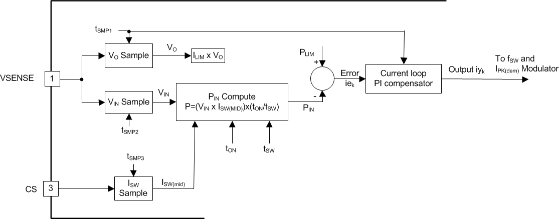
In addition to the peak-current mode PWM function, the device also uses sensed current at the CS pin to estimate the secondary-side load current. The device samples the CS pin voltage and measures it in the middle of the on-time, which is effectively the average switch current during the on time, ISW(avg_on). This measurement scheme is the case during both DCM and CCM operational modes. The average switch current during the on time is scaled by the PWM duty cycle to give the IIN(avg) of the power stage. The power stage input power, PIN, can then be estimated as the product of (VIN x IIN(avg)). The CC mode operation regulates PIN to track (IOUT(lim) x VOUT), if PIN increases to reach PIN(lim), thereby achieving a regulated constant current as shown in Equation 18.


 Figure 33. Digital Current Control Loop Simplified Block Diagram
 Assuming that the power stage efficiency does not change significantly with operating point, by regulating the input power in inverse proportion to output voltage, this regulates output current. This achieves a brick-wall CC characteristic, where the output current is regulated as the input voltage changes and as the output voltage rolls off, regardless of power stage operating mode (CCM or DCM). The CC mode protection eliminates the characteristic load current tail-out that is typically seen with peak-current mode control as output voltage collapses and operation goes deeper into CCM mode.
NOTE
As the output voltage decreases in CC mode, the VDD level also decreases. If the overload is severe, the drop in output voltage causes VDD to drop below the VDD(stop) UV level. This drop causes a shutdown for tRESET(long), as given in Table 7, followed by a restart attempt.
The constant-current mode output current limit level (IOUT(lim)) is a function of both the RCS1 resistor and the transformer turns ratio. The device uses an internal reference and gain for the CC loop, KCC1 and KCC2, that set the CC IOUT(lim) point as a function of the chosen turns ratio, output voltage and current sense resistance as shown in Equation 20.

For the UCC28631, UCC28632 and the UCC28633 devices, the IOUT(lim) can be adjusted to be a percentage of the maximum value calculated by equation Equation 20. see CC-Mode IOUT(lim) Adjustment for more details.