ZHCSC62D March 2014 – December 2017 UCC28630 , UCC28631 , UCC28632 , UCC28633 , UCC28634
PRODUCTION DATA.
- 1 特性
- 2 应用
- 3 说明
- 4 修订历史记录
- 5 Device Comparison Table
- 6 Pin Configuration and Functions
- 7 Specifications
-
8 Detailed Description
- 8.1 Overview
- 8.2 Functional Block Diagram
- 8.3
Feature Description
- 8.3.1 High-Voltage Current Source Start-Up Operation
- 8.3.2 AC Input UVLO / Brownout Protection
- 8.3.3 Active X-Capacitor Discharge (UCC28630 and UCC28633 only)
- 8.3.4 Magnetic Input and Output Voltage Sensing
- 8.3.5 Fixed-Point Magnetic Sense Sampling Error Sources
- 8.3.6 Magnetic Sense Resistor Network Calculations
- 8.3.7 Magnetic Sensing: Power Stage Design Constraints
- 8.3.8 Magnetic Sense Voltage Control Loop
- 8.3.9 Peak Current Mode Control
- 8.3.10 IPEAK Adjust vs. Line
- 8.3.11 Primary-Side Constant-Current Limit (CC Mode)
- 8.3.12 Primary-Side Overload Timer (UCC28630 only)
- 8.3.13 Overload Timer Adjustment (UCC28630 only)
- 8.3.14 CC-Mode IOUT(lim) Adjustment
- 8.3.15 Fault Protections
- 8.3.16 Pin-Fault Detection and Protection
- 8.3.17 Over-Temperature Protection
- 8.3.18 External Fault Input
- 8.3.19 External SD Pin Wake Input (except UCC28633)
- 8.3.20 External Wake Input at VSENSE Pin (UCC28633 Only)
- 8.3.21 Mode Control and Switching Frequency Modulation
- 8.3.22 Frequency Dither For EMI (except UCC28632)
- 8.4 Device Functional Modes
-
9 Applications and Implementation
- 9.1 Application Information
- 9.2
Typical Application
- 9.2.1 Notebook Adapter, 19.5 V, 65 W
- 9.2.2 UCC28630 Application Schematic
- 9.2.3 Design Requirements
- 9.2.4
Detailed Design Procedure
- 9.2.4.1 Custom Design With WEBENCH® Tools
- 9.2.4.2 Input Bulk Capacitance and Minimum Bulk Voltage
- 9.2.4.3 Transformer Turn Ratio
- 9.2.4.4 Transformer Magnetizing Inductance
- 9.2.4.5 Current Sense Resistor RCS
- 9.2.4.6 Transformer Constraint Verification
- 9.2.4.7 Transformer Selection and Design
- 9.2.4.8 Slope Compensation Verification
- 9.2.4.9 Power MOSFET and Output Rectifier Selection
- 9.2.4.10 Output Capacitor Selection
- 9.2.4.11 Calculation of CC Mode Limit Point
- 9.2.4.12 VDD Capacitor Selection
- 9.2.4.13 Magnetic Sense Resistor Network Selection
- 9.2.4.14 Output LED Pre-Load Resistor Calculation
- 9.2.5 External Wake Pulse Calculation at VSENSE Pin (UCC28633 Only)
- 9.2.6 Energy Star Average Efficiency and Standby Power
- 9.2.7 Application Performance Plots
- 9.3 Dos and Don'ts
- 10Power Supply Recommendations
- 11Layout
- 12器件和文档支持
- 13机械、封装和可订购信息
8.3.19 External SD Pin Wake Input (except UCC28633)
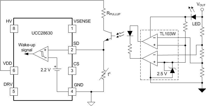
During low-power modes (when fSW < fSMP(max)), the device disables the internal pull-up on the SD pin. This action allows the pin voltage to fall to GND, and the SD pin then functions as a transient wake-up input. In this case, if the pin rises above the wake threshold while the device is in low-power sleep mode, the device wakes and starts PWM pulses immediately. This feature is useful for applications that require a faster response to load transients from zero or near-zero load, where a wake-up signal can be appropriately coupled to the SD pin from the secondary side.
Figure 38 describes a typical secondary-side wake circuit and coupling of the wake signal to the controller on the primary side. This circuit uses a TL103W component which is an integrated reference plus two op-amps in a convenient SOIC-8 package. Both op-amps are connected to the same internal 2.5-V TL431 type reference, with a 3-resistor divider chain allowing each op-amp to monitor a different level. The upper op-amp output is low as long as the device is regulating the output voltage normally. If a sufficiently large load transient occurs while the primary-side controller is in sleep mode, the output voltage drops below a transient wake level. The upper op-amp output goes high, driving current through the low-cost wake signal opto-coupler. On the primary side, the wake opto-coupler pulls up the SD pin above the wake threshold and forces PWM switching as a reaction to the load transient.
The lower op-amp section monitors the output voltage and its output goes low only when the output voltage is above a minimum enable threshold for the secondary-side wake-up monitor. This action is necessary so that under certain conditions, such as a start-up sequence or short-circuit condition (when the output voltage is already below the transient wake level) that the secondary-side circuit does not continually drive the wake opto-coupler, which could activate an SD pin fault during pin-fault checking at start-up.
 Figure 38. Typical Secondary-Side Voltage Monitor and Wake-Up Circuit for Interfacing to the SD Pin