ZHCSCE8F April 2014 – May 2019 TPD1S514
PRODUCTION DATA.
- 1 特性
- 2 应用
- 3 说明
- 4 修订历史记录
- 5 Device Comparison Table
- 6 Pin Configuration and Functions
-
7 Specifications
- 7.1 Absolute Maximum Ratings
- 7.2 ESD Ratings
- 7.3 Recommended Operating Conditions
- 7.4 Thermal Information
- 7.5 Supply Current Consumption
- 7.6 Electrical Characteristics EN Pin
- 7.7 Thermal Shutdown Feature
- 7.8 Electrical Characteristics nFET Switch
- 7.9 Electrical Characteristics OVP Circuit
- 7.10 Electrical Characteristics VBUS_POWER Circuit
- 7.11 Timing Requirements
- 7.12 TPD1S514-1 Typical Characteristics
-
8 Detailed Description
- 8.1 Overview
- 8.2 Functional Block Diagram
- 8.3
Feature Description
- 8.3.1 Over Voltage Protection on VBUS_CON up to 30 V DC
- 8.3.2 Precision OVP (< ±1% Tolerance)
- 8.3.3 Low RON nFET Switch Supports Host and Charging Mode
- 8.3.4 VBUS_POWER, TPD1S514-1, TPD1S514-2, TPD1S514-3
- 8.3.5 VBUS_POWER, TPD1S514
- 8.3.6 Powering the System When Battery is Discharged
- 8.3.7 ±15 kV IEC 61000-4-2 Level 4 ESD Protection
- 8.3.8 100 V IEC 61000-4-5 µs Surge Protection
- 8.3.9 Startup and OVP Recovery Delay
- 8.3.10 Thermal Shutdown
- 8.4 Device Functional Modes
- 9 Application and Implementation
- 10Power Supply Recommendations
- 11Layout
- 12器件和文档支持
- 13机械、封装和可订购信息
7.11 Timing Requirements
over operating free-air temperature range (unless otherwise noted)| PARAMETER | TEST CONDITIONS | MIN | TYP | MAX | UNIT | ||
|---|---|---|---|---|---|---|---|
| tDELAY | USB charging turn-ON Delay | Measured from EN asserted LOW to nFET begins to Turn ON, excludes soft-start time | TPD1S514-1 | 20 | ms | ||
| TPD1S514-2 | |||||||
| TPD1S514-3 | |||||||
| TPD1S514 | |||||||
| tSS | USB charging rise time (soft-start delay) | Force 5 V on VBUS_CON, measured from VBUS_SYS rises from 10% to 90% (with 1 MΩ load/ NO CLOAD) | TPD1S514-1 | 3.5 | ms | ||
| TPD1S514-2 | |||||||
| TPD1S514-3 | |||||||
| TPD1S514 | |||||||
| tOFF_DELAY | USB charging turn-OFF time | Measured from EN asserted High to VBUS_SYS falling to 10% with RLOAD = 10 Ω and No CLOAD on VBUS_SYS | TPD1S514-1 | 5.5 | µs | ||
| TPD1S514-2 | |||||||
| TPD1S514-3 | |||||||
| TPD1S514 | |||||||
| OVER VOLTAGE PROTECTION | |||||||
| tOVP_response | OVP response time | Measured from OVP Condition to FET Turn OFF(1) | 100 | ns | |||
(1) Specified by design, not production tested
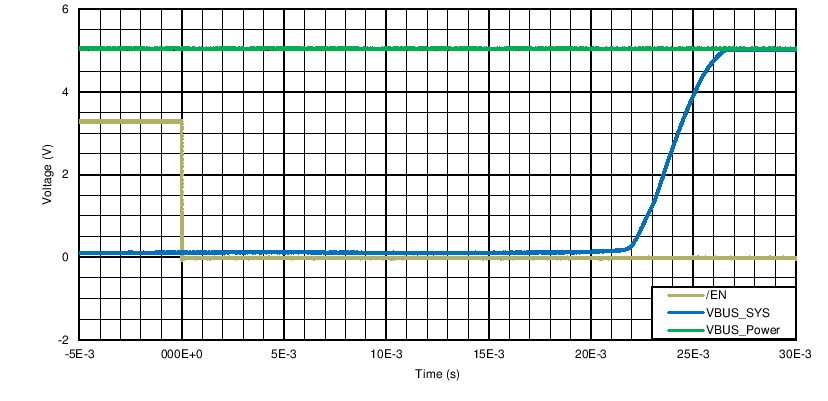
 Figure 1. TPD1S514-1 Response to Set EN Low