ZHCSCH4H June 2013 – November 2016 TPS65132 , TPS65132S
UNLESS OTHERWISE NOTED, this document contains PRODUCTION DATA.
- 1 特性
- 2 应用范围
- 3 说明
- 4 修订历史记录
- 5 Device Comparison Table
- 6 Pin Configuration and Functions
- 7 Specifications
- 8 Detailed Description
-
9 Application and Implementation
- 9.1 Application Information
- 9.2
Typical Applications
- 9.2.1
Low-current Applications (≤ 40 mA)
- 9.2.1.1 Design Requirements
- 9.2.1.2 Detailed Design Procedure
- 9.2.1.3 Application Curves
- 9.2.2
Mid-current Applications (≤ 80 mA)
- 9.2.2.1 Design Requirements
- 9.2.2.2 Detailed Design Procedure
- 9.2.2.3 Application Curves
- 9.2.3 High-current Applications (≤ 150 mA)
- 9.2.1
Low-current Applications (≤ 40 mA)
- 10Power Supply Recommendations
- 11Layout
- 12器件和文档支持
- 13机械、封装和可订购信息
9 Application and Implementation
NOTE
Information in the following applications sections is not part of the TI component specification, and TI does not warrant its accuracy or completeness. TI’s customers are responsible for determining suitability of components for their purposes. Customers should validate and test their design implementation to confirm system functionality.
9.1 Application Information
The TPS65132xx devices, primarily intended to supplying TFT LCD displays, can be used for any application that requires positive and negative supplies, ranging from ±4 V to ±6 V and current up to 80 mA (150 mA for the TPS65132Sx version). Both output voltages can be set independently and their sequencing is also independent. The following section presents the different operating modes that the device can support as well as the different features that the user can select.
9.2 Typical Applications
9.2.1 Low-current Applications (≤ 40 mA)
The TPS65132 can be programmed to 40mA mode with the APPS bit to support applications that require output currents up to 40 mA (refer to Figure 17). The 40mA mode limits the negative charge pump output current to 40 mA DC in order to provide the highest efficiency possible. The VPOS rail can deliver up to 200 mA DC regardless of the mode. Output peak currents are supported by the output capacitors.
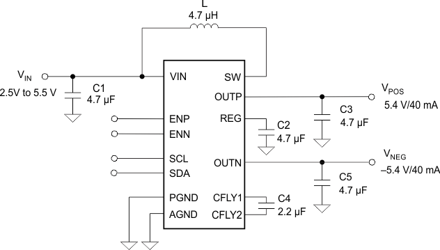 Figure 19. Typical Low-current Application Circuit
9.2.1.1 Design Requirements
Table 8. Design Parameters
| PARAMETERS | EXAMPLE VALUES |
|---|---|
| Input Voltage Range | 2.5 V to 5.5 V |
| Output Voltages | 4.0 V to 6.0 V, –4.0 V to –6.0 V |
| Output Current Rating | 40 mA |
| Boost Converter Switching Frequency | 1.8 MHz |
| Negative Charge Pump Switching Frequency | 1.0 MHz |
9.2.1.2 Detailed Design Procedure
9.2.1.2.1 Sequencing
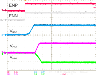
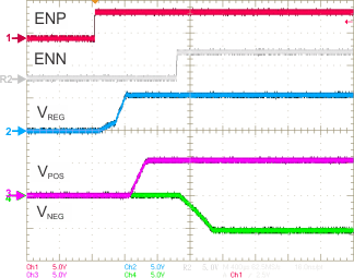
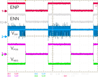
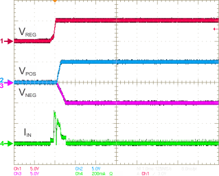
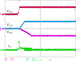
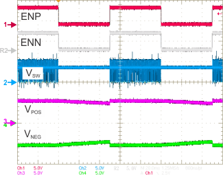
Each output rail (VPOS and VNEG) is enabled and disabled using an external enable signal. If not explicitly specified, the enable signal in the rest of the document refers to ENN or ENP: ENP for the positive rail VPOS and ENN for the negative rail VNEG. Figure 33 to Figure 36 show the typical sequencing waveforms.
NOTE
In the case where VIN falls below the UVLO threshold while one of the enable signals is still high, all converters will be shut down instantaneously and both VPOS and VNEG output rails will be actively discharged to GND.
9.2.1.2.2 Boost Converter Design Procedure
The first step in the design procedure is to verify whether the maximum possible output current of the boost converter supports the specific application requirements. A simple approach is to estimate the converter efficiency, by taking the efficiency number from the provided efficiency curves at the application's maximum load or to use a worst case assumption for the expected efficiency, e.g., 85%.
- Duty Cycle:

- Inductor ripple current:

- Maximum output current:

- Peak switch current of the application:

η = Estimated boost converter efficiency (use the number from the efficiency plots or 85% as an estimation)
ƒSW = Boost converter switching frequency (1.8 MHz)
L = Selected inductor value for the boost converter (see the Inductor Selection section)
ISWPEAK = Boost converter switch current at the desired output current (must be < [ ILIM_min + ΔIL])
ΔIL = Inductor peak-to-peak ripple current
VREG = max (VPOS, |VNEG|) + 200 mV (in 40mA mode — + 300 mV in 80mA mode — + 500 mV with TPS65132Sx with SYNC = HIGH)
IOUT = IOUT_VPOS + | IOUT_VNEG| (IOUT_max being the maximum current delivered on each rail)
The peak switch current is the current that the integrated switch and the inductor have to handle. The calculation must be done for the minimum input voltage where the peak switch current is highest.
9.2.1.2.2.1 Inductor Selection (Boost Converter)
Saturation current: the inductor must handle the maximum peak current (IL_SAT > ISWPEAK, or IL_SAT > [ ILIM_min + ΔIL] as conservative approach)
DC Resistance: the lower the DCR, the lower the losses
Inductor value: in order to keep the ratio IOUT/ΔIL low enough for proper sensing operation purpose, it is recommended to use a 4.7 µH inductor for 40mA mode (a 2.2 µH might however be used, but the efficiency might be lower than with 4.7 µH at light loads depending on the inductor characteristics).
Table 9. Inductor Selection Boost(1)
| L (µH) |
SUPPLIER(1) | COMPONENT CODE | EIA SIZE | DCR TYP (mΩ) |
ISAT
(A) |
|---|---|---|---|---|---|
| 2.2 | Toko | 1269AS-H-2R2N=P2 | 1008 | 130 | 2.4 |
| 2.2 | Murata | LQM2HPN2R2MG0 | 1008 | 80 | 1.3 |
| 2.2 | Murata | LQM21PN2R2NGC | 0805 | 250 | 0.8 |
| 4.7 | Toko | 1269AS-H-4R7N=P2 | 1008 | 250 | 1.6 |
| 4.7 | Murata | LQM21PN4R7MGR | 0805 | 230 | 0.8 |
| 4.7 | FDK | MIPS2520D4R7 | 1008 | 280 | 0.7 |
9.2.1.2.2.2 Input Capacitor Selection (Boost Converter)
For best input voltage filtering low ESR ceramic capacitors are recommended. TPS65132 has an analog input pin VIN. A 4.7 µF minimum bypass capacitor is required as close as possible from VIN to GND. This capacitor is also used as the boost converter input capacitor.
For better input voltage filtering, this value can be increased or two capacitors can be used: one 4.7 µF input capacitor for the boost converter as well as a 1 µF bypass capacitor close to the VIN pin. Refer to the Recommended Operating Conditions, Table 10 and Figure 19 for input capacitor recommendations.
9.2.1.2.2.3 Output Capacitor Selection (Boost Converter)
For the best output voltage filtering, low-ESR ceramic capacitors are recommended. A minimum of 4.7 µF ceramic output capacitor is required. Higher capacitor values can be used to improve the load transient response. Refer to the Recommended Operating Conditions, Table 10 and Figure 19 for output capacitor recommendations.
Table 10. Input And Output Capacitor Selection(1)
| CAPACITOR (µF) |
SUPPLIER | COMPONENT CODE | EIA SIZE (Thickness max.) | VOLTAGE RATING (V) |
COMMENTS |
|---|---|---|---|---|---|
| 2.2 | Murata | GRM188R61C225KAAD | 0603 (0.9 mm) | 16 | CFLY |
| 4.7 | Murata | GRM188R61C475KAAJ | 0603 (0.95 mm) | 16 | CIN, CNEG, CPOS, CREG |
| 10 | Murata | GRM219R61C106KA73 | 0603 (0.95 mm) | 16 | CNEG, CREG |
9.2.1.2.3 Input Capacitor Selection (LDO)
The LDO input capacitor is also the boost converter output capacitor. Refer to the Recommended Operating Conditions, Table 10 and Figure 19.
9.2.1.2.4 Output Capacitor Selection (LDO)
The LDO is designed to operate with a 4.7 µF minimum ceramic output capacitor. Refer to the Recommended Operating Conditions, Table 10 and Figure 19.
9.2.1.2.5 Input Capacitor Selection (CPN)
The CPN input capacitor is also the boost converter output capacitor. Refer to the Recommended Operating Conditions, Table 10 and Figure 19.
9.2.1.2.6 Output Capacitor Selection (CPN)
The CPN is designed to operate with a 4.7 µF minimum ceramic output capacitor. Refer to the Recommended Operating Conditions, Table 10 and Figure 19.
9.2.1.2.7 Flying Capacitor Selection (CPN)
The CPN needs an external flying capacitor. The minimum value is 2.2 µF. Special care must be taken while choosing the flying capacitor as it will directly impact the output voltage accuracy and load regulation performance. Therefore, a minimum capacitance of 1 µF must be achieved by the capacitor at a DC bias voltage of │VNEG│ + 300 mV. For proper operation, the flying capacitor value must be lower than the output capacitor of the boost converter on REG pin.
9.2.1.3 Application Curves
VIN = 3.7 V, VPOS = 5.4 V, VNEG = –5.4 V, unless otherwise notedTable 11. Component List Used For The Application Curves
| REFERENCE | DESCRIPTION | MANUFACTURER AND PART NUMBER(1) |
|---|---|---|
| C | 2.2 µF, 16 V, 0603, X5R, ceramic | Murata - GRM188R61C225KAAD |
| 4.7 µF, 16 V, 0603, X5R, ceramic | Murata - GRM188R61C475KAAJ | |
| 10 μF, 16 V, 0603, X5R, ceramic | Murata - GRM188R61E106MA73 | |
| L | 2.2 µH, 2.4 A, 130 mΩ, 2.5 mm × 2.0 mm × 1.0 mm | Toko - DFE252010C (1269AS-H-2R2N=P2) |
| 4.7 µH, 1.6 A, 250 mΩ, 2.5 mm × 2.0 mm × 1.0 mm | Toko - DFE252010C (1269AS-H-4R7N=P2) | |
| U1 | TPS65132AYFF | Texas Instruments |
Table 12. Table Of Graphs
| PARAMETER | CONDITIONS | Figure |
|---|---|---|
| EFFICIENCY | ||
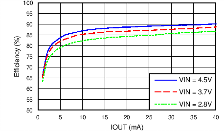
| Efficiency vs. Output Current | ± 5.0 V — 40mA Mode — L = 4.7 µH | Figure 20 |
| Efficiency vs. Output Current | ± 5.4 V — 40mA Mode — L = 4.7 µH | Figure 21 |
| Efficiency vs. Output Current | ± 5.0 V — 40mA Mode — L = 2.2 µH | Figure 22 |
| Efficiency vs. Output Current | ± 5.4 V — 40mA Mode — L = 2.2 µH | Figure 23 |
| CONVERTERS WAVEFORMS | ||
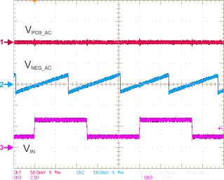
| VNEG Output Ripple | INEG = 2 mA / 20 mA / 40 mA — 40mA Mode — COUT = 4.7 µF | Figure 24 |
| VNEG Output Ripple | INEG = 2 mA / 20 mA / 40 mA — 40mA Mode — COUT = 2 × 4.7 µF | Figure 25 |
| VPOS Output Ripple | Any load | Figure 26 |
| LOAD TRANSIENT | ||
| Load Transient | VIN = 2.9 V — IPOS = –INEG = 5 mA → 35 mA → 5 mA — 40mA Mode — L = 4.7 µH | Figure 27 |
| Load Transient | VIN = 3.7 V — IPOS = –INEG = 5 mA → 35 mA → 5 mA — 40mA Mode — L = 4.7 µH | Figure 28 |
| Load Transient | VIN = 4.5 V — IPOS = –INEG = 5 mA → 35 mA → 5 mA — 40mA Mode — L = 4.7 µH | Figure 29 |
| LINE TRANSIENT | ||
| Line Transient | VIN = 2.8 V → 4.5 V → 2.8 V — IPOS = –INEG = 0 mA — 40mA Mode — L = 4.7 µH | Figure 30 |
| Line Transient | VIN = 2.8 V → 4.5 V → 2.8 V — IPOS = –INEG = 5 mA — 40mA Mode — L = 4.7 µH | Figure 31 |
| Line Transient | VIN = 2.8 V → 4.5 V → 2.8 V — IPOS = –INEG = 35 mA — 40mA Mode — L = 4.7 µH | Figure 32 |
| POWER SEQUENCING | ||
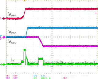
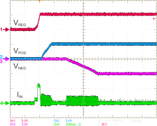
| Power-up Sequencing | Simultaneous — no load | Figure 33 |
| Power-down Sequencing | Simultaneous — no load with Active Discharge | Figure 34 |
| Power-up Sequencing | Sequential — no load | Figure 35 |
| Power-down Sequencing | Sequential — no load with Active Discharge | Figure 36 |
| Power-up/down Sequencing | Simultaneous — no load with Active Discharge | Figure 37 |
| Power-up/down Sequencing | Simultaneous — no load without Active Discharge | Figure 38 |
| INRUSH CURRENT | ||
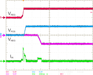
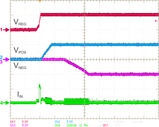
| Inrush Current | Simultaneous — no load — 40mA Mode | Figure 39 |
| Inrush Current | Sequential — no load — 40mA Mode | Figure 40 |
| Inrush Current | Simultaneous — no load — 40mA Mode — TPS65132B2, –Lx, –Sx, –Tx, –Wx | Figure 41 |
| Inrush Current | Sequential — no load — 40mA Mode — TPS65132B2, –Lx, –Sx, –Tx, –Wx | Figure 42 |
| LOAD REGULATION | ||
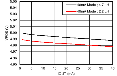
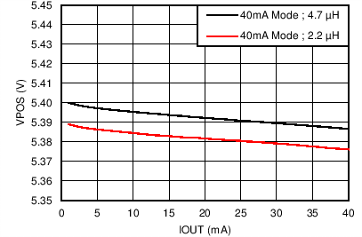
| VPOS vs Output Current | VPOS = 5.0 V — 40mA Mode — IPOS = 0 mA to 40 mA — L = 4.7 µH and 2.2 µH | Figure 43 |
| VPOS vs Output Current | VPOS = 5.4 V — 40mA Mode — IPOS = 0 mA to 40 mA — L = 4.7 µH and 2.2 µH | Figure 44 |
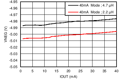
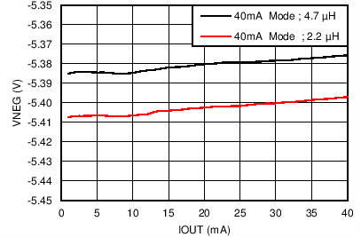
| VNEG vs Output Current | VNEG = –5.0 V — 40mA Mode — INEG = 0 mA to 40 mA — L = 4.7 µH and 2.2 µH | Figure 45 |
| VNEG vs Output Current | VNEG = –5.4 V — 40mA Mode — INEG = 0 mA to 40 mA — L = 4.7 µH and 2.2 µH | Figure 46 |
| LINE REGULATION | ||
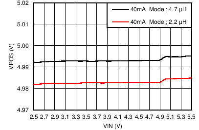
| VPOS vs Output Voltage | VIN = 2.5 V to 5.5 V — VPOS = 5.0 V — 40mA Mode — IPOS = 20 mA — L = 4.7 µH and 2.2 µH | Figure 47 |
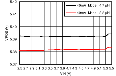
| VPOS vs Output Voltage | VIN = 2.5 V to 5.5 V — VPOS = 5.4 V — 40mA Mode — IPOS = 20 mA — L = 4.7 µH and 2.2 µH | Figure 48 |
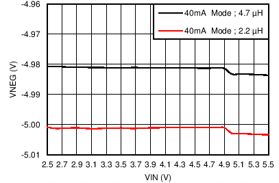
| VNEG vs Output Voltage | VIN = 2.5 V to 5.5 V — VNEG = –5.0 V — 40mA Mode — INEG = 20 mA — L = 4.7 µH and 2.2 µH | Figure 49 |
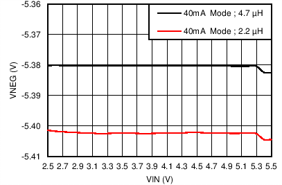
| VNEG vs Output Voltage | VIN = 2.5 V to 5.5 V — VNEG = –5.4 V — 40mA Mode — INEG = 20 mA — L = 4.7 µH and 2.2 µH | Figure 50 |
spacer
NOTE
In this section, IOUT means that the outputs are loaded with IPOS = –INEG simultaneously.
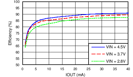
| ± 5.0 V | L = 4.7 µH |
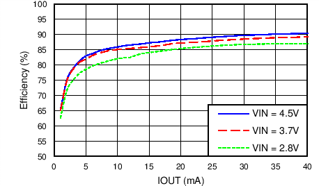
| ± 5.4 V | L = 4.7 µH |
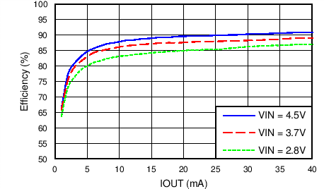
| ± 5.0 V | L = 2.2 µH |
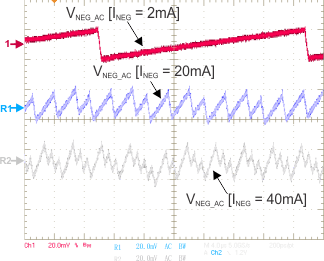
| L = 4.7 µH | COUT = 4.7 µF |
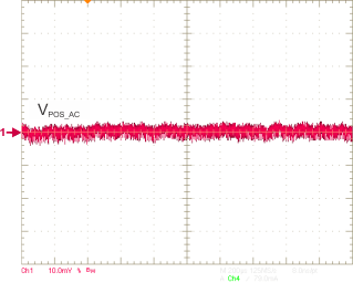
| ± 5.4 V | L = 2.2 µH |
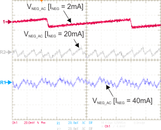
| L = 4.7 µH | COUT = 2 × 4.7 µF |
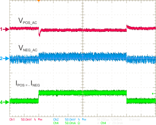
| VIN = 2.9 V | ΔIOUT = 30 mA |
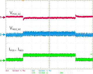
| VIN = 4.5 V | ΔIOUT = 30 mA |
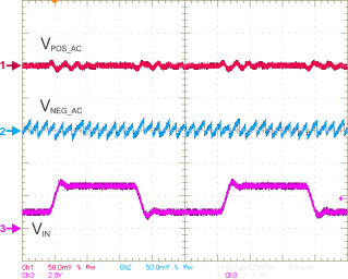
| IOUT = 5 mA | ΔVIN = 1.7 V |

| VIN = 3.7 V | ΔIOUT = 30 mA |
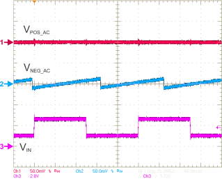
| IOUT = 0 mA | ΔVIN = 1.7 V |
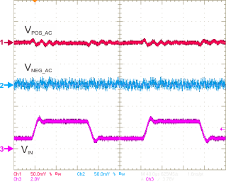
| IOUT = 35 mA | ΔVIN = 1.7 V |
(TPS65132B2, –Lx, –Sx, –Tx, –Wx)
| VPOS = 5 V |
| VNEG = –5 V |
| VPOS = 5 V |
| VNEG = –5 V |
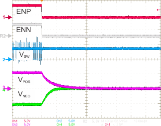
(with Active Discharge)
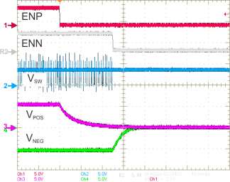
(with Active Discharge)
(TPS65132Ax only)
(TPS65132B2, –Lx, –Sx, –Tx, –Wx)
| VPOS = 5.4 V |
| VNEG = –5.4 V |
| VPOS = 5.4 V |
| VNEG = –5.4 V |
9.2.2 Mid-current Applications (≤ 80 mA)
The TPS65132 can be programmed to 80mA mode with the APPS bit to support applications that require output currents up to 80 mA (refer to Figure 17). The 80mA mode is limiting the negative charge pump (CPN) output current to 80 mA DC in order to provide the highest efficiency possible where the V(POS) rail can deliver up to 200 mA DC regardless of the mode. Output peak currents are supported by the output capacitors.
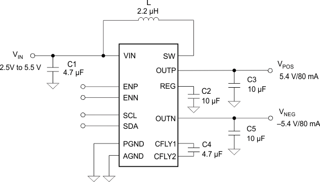 Figure 51. Typical Mid-current Application Circuit
9.2.2.1 Design Requirements
Table 13. Design Parameters
| PARAMETERS | EXAMPLE VALUES |
|---|---|
| Input Voltage Range | 2.5 V to 5.5 V |
| Output Voltages | 4.0 V to 6.0 V, –4.0 V to –6.0 V |
| Output Current Rating | 80 mA |
| Boost Converter Switching Frequency | 1.8 MHz |
| Negative Charge Pump Switching Frequency | 1.0 MHz |
9.2.2.2 Detailed Design Procedure
The design procedure for the mid-current applications (80mA mode) is identical to the one for the low-current applications (40mA mode), except for the BOM (bill of materials). Refer to the Detailed Design Procedure for details about the sequencing and the general component selection.
9.2.2.2.1 Boost Converter Design Procedure
9.2.2.2.1.1 Inductor Selection (Boost Converter)
In order to keep the ratio IOUT/ΔIL low enough for proper sensing operation purpose, it is recommended to use a 2.2 µH inductor for 80mA mode. For details, see Inductor Selection (Boost Converter).
9.2.2.2.1.2 Input Capacitor Selection (Boost Converter)
A 4.7 µF minimum bypass capacitor is required as close as possible from VIN to GND. This capacitor is also used as the boost converter input capacitor.
For better input voltage filtering, this value can be increased or two capacitors can be used: one 4.7 µF input capacitor for the boost converter as well as a 1 µF bypass capacitor close to the VIN pin. Refer to the Recommended Operating Conditions, Table 10 and Figure 51 for input capacitor recommendations.
9.2.2.2.1.3 Output Capacitor Selection (Boost Converter)
For best output voltage filtering low ESR ceramic capacitors are recommended. A minimum of 10 µF ceramic output capacitor is required. Higher capacitor values can be used to improve the load transient response. Refer to the Recommended Operating Conditions, Table 10 and Figure 51 for output capacitor recommendations.
9.2.2.2.2 Input Capacitor Selection (LDO)
The LDO input capacitor is also the boost converter output capacitor. Refer to the Recommended Operating Conditions, Table 10 and Figure 51.
9.2.2.2.3 Output Capacitor Selection (LDO)
The LDO is designed to operate with a 4.7 µF minimum ceramic output capacitor. Refer to the Recommended Operating Conditions, Table 10 and Figure 51.
9.2.2.2.4 Input Capacitor Selection (CPN)
The CPN input capacitor is also the boost converter output capacitor. Refer to the Recommended Operating Conditions, Table 10 and Figure 51.
9.2.2.2.5 Output Capacitor Selection (CPN)
The CPN is designed to operate with a 10 µF minimum ceramic output capacitor. Refer to the Recommended Operating Conditions, Table 10 and Figure 51.
9.2.2.2.6 Flying Capacitor Selection (CPN)
The CPN needs an external flying capacitor. The minimum value is 4.7 µF. Special care must be taken while choosing the flying capacitor as it will directly impact the output voltage accuracy and load regulation performance. Therefore, a minimum capacitance of 2.2 µF must be achieved by the capacitor at a DC bias voltage of │VNEG│ + 300 mV. For proper operation, the flying capacitor value must be lower than the output capacitor of the boost converter on REG pin.
9.2.2.3 Application Curves
VIN = 3.7 V, VPOS = 5.4 V, VNEG = –5.4 V, unless otherwise notedTable 14. Component List For Typical Characteristics Circuits
| REFERENCE | DESCRIPTION | MANUFACTURER AND PART NUMBER(1) |
|---|---|---|
| C | 2.2 µF, 16 V, 0603, X5R, ceramic | Murata - GRM188R61C225KAAD |
| 4.7 µF, 16 V, 0603, X5R, ceramic | Murata - GRM188R61C475KAAJ | |
| 10 μF, 16 V, 0603, X5R, ceramic | Murata - GRM188R61E106MA73 | |
| L | 2.2 µH, 2.4 A, 130 mΩ, 2.5 mm × 2.0 mm × 1.0 mm | Toko - DFE252010C (1269AS-H-2R2N=P2) |
| U1 | TPS65132AYFF | Texas Instruments |
Table 15. Table Of Graphs
| PARAMETER | CONDITIONS | Figure |
|---|---|---|
| EFFICIENCY | ||
| Efficiency vs. Output Current | ± 5.0 V — 80mA Mode — L = 2.2 µH | Figure 52 |
| Efficiency vs. Output Current | ± 5.4 V — 80mA Mode — L = 2.2 µH | Figure 53 |
| CONVERTERS WAVEFORMS | ||
| VNEG Output Ripple | INEG = 4 mA / 40 mA / 80 mA — 80mA Mode — COUT = 10 µF | Figure 54 |
| VNEG Output Ripple | INEG = 4 mA / 40 mA / 80 mA — 80mA Mode — COUT = 2 × 10 µF | Figure 55 |
| VPOS Output Ripple | IPOS = 150 mA — 80mA Mode | Figure 56 |
| LOAD TRANSIENT | ||
| Load Transient | VIN = 2.9 V — IPOS = –INEG = 10 mA → 70 mA → 10 mA — 80mA Mode — L = 2.2 µH | Figure 57 |
| Load Transient | VIN = 3.7 V — IPOS = –INEG = 10 mA → 70 mA → 10 mA — 80mA Mode — L = 2.2 µH | Figure 58 |
| Load Transient | VIN = 4.5 V — IPOS = –INEG = 10 mA → 70 mA → 10 mA — 80mA Mode — L = 2.2 µH | Figure 59 |
| LINE TRANSIENT | ||
| Line Transient | VIN = 2.8 V → 4.5 V → 2.8 V — IPOS = –INEG = 0 mA — 80mA Mode — L = 2.2 µH | Figure 60 |
| Line Transient | VIN = 2.8 V → 4.5 V → 2.8 V — IPOS = –INEG = 40 mA — 80mA Mode — L = 2.2 µH | Figure 61 |
| Line Transient | VIN = 2.8 V → 4.5 V → 2.8 V — IPOS = –INEG = 70 mA — 80mA Mode — L = 2.2 µH | Figure 62 |
| POWER SEQUENCING | ||
| Power-up Sequencing | Simultaneous — no load | Figure 63 |
| Power-down Sequencing | Simultaneous — no load with Active Discharge | Figure 64 |
| Power-up Sequencing | Sequential — no load | Figure 65 |
| Power-down Sequencing | Sequential — no load with Active Discharge | Figure 66 |
| Power-up/down Sequencing | Simultaneous — no load with Active Discharge | Figure 67 |
| Power-up/down Sequencing | Simultaneous — no load without Active Discharge | Figure 68 |
| INRUSH CURRENT | ||
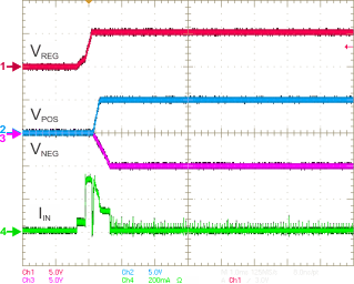
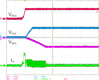
| Inrush Current | Simultaneous — no load — 80mA Mode | Figure 69 |
| Inrush Current | Sequential — no load — 80mA Mode | Figure 70 |
| Inrush Current | Simultaneous — no load — 80mA Mode — TPS65132B2, –Lx, –Sx, –Tx, –Wx | Figure 71 |
| Inrush Current | Sequential — no load — 80mA Mode — TPS65132B2, –Lx, –Sx, –Tx, –Wx | Figure 72 |
| LOAD REGULATION | ||
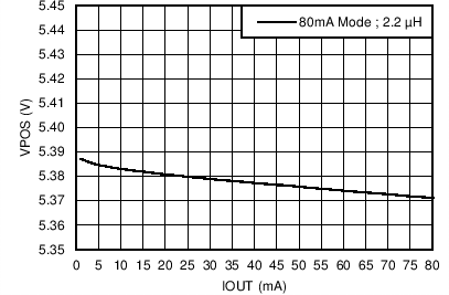
| VPOS vs Output Current | VPOS = 5.0 V — 80mA Mode — IPOS = 0 mA to 80 mA — L = 2.2 µH | Figure 73 |
| VPOS vs Output Current | VPOS = 5.4 V — 80mA Mode — IPOS = 0 mA to 80 mA — L = 2.2 µH | Figure 74 |
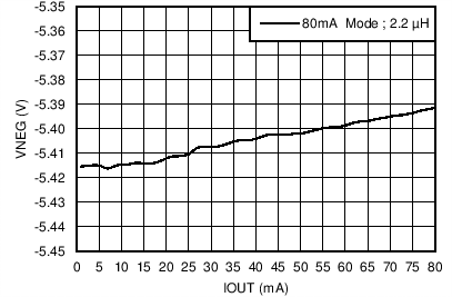
| VNEG vs Output Current | VNEG = –5.0 V — 80mA Mode — INEG = 0 mA to 80 mA — L = 2.2 µH | Figure 75 |
| VNEG vs Output Current | VNEG = –5.4 V — 80mA Mode — INEG = 0 mA to 80 mA — L = 2.2 µH | Figure 76 |
| LINE REGULATION | ||
| VPOS vs Output Voltage | VIN = 2.5 V to 5.5 V — VPOS = 5.0 V — 80mA Mode — IPOS = 60 mA — L = 2.2 µH | Figure 77 |
| VPOS vs Output Voltage | VIN = 2.5 V to 5.5 V — VPOS = 5.4 V — 80mA Mode — IPOS = 60 mA — L = 2.2 µH | Figure 78 |
| VNEG vs Output Voltage | VIN = 2.5 V to 5.5 V — VNEG = –5.0 V — 80mA Mode — INEG = 60 mA — L = 2.2 µH | Figure 79 |
| VNEG vs Output Voltage | VIN = 2.5 V to 5.5 V — VNEG = –5.4 V — 80mA Mode — INEG = 60 mA — L = 2.2 µH | Figure 80 |
spacer
NOTE
In this section, IOUT means that the outputs are loaded with IPOS = –INEG simultaneously.
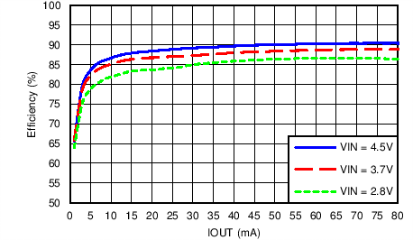
| ± 5 V | L = 2.2 µH |
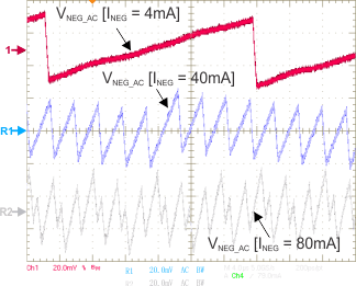
| L = 2.2 µH | COUT = 10 µF |

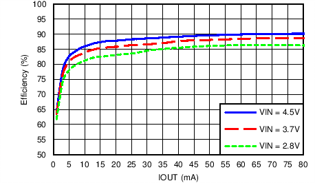
| ± 5.4 V | L = 2.2 µH |
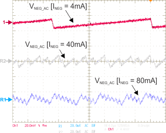
| L = 2.2 µH | COUT = 2 × 10 µF |
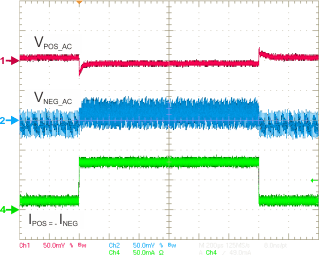
| VIN = 2.9 V | ΔIOUT = 60 mA |
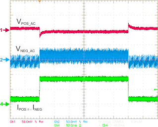
| VIN = 4.5 V | ΔIOUT = 60 mA |
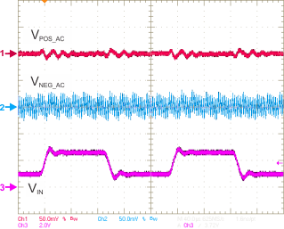
| IOUT = 40 mA | ΔVIN = 1.7 V |
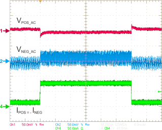
| VIN = 3.7 V | ΔIOUT = 60 mA |
| IOUT = 0 mA | ΔVIN = 1.7 V |
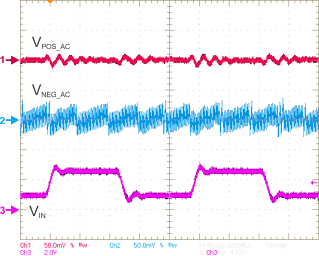
| IOUT = 70 mA | ΔVIN = 1.7 V |


(TPS65132B2, –Lx, –Sx, –Wx)
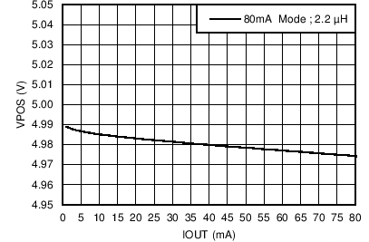
| VPOS = 5 V |
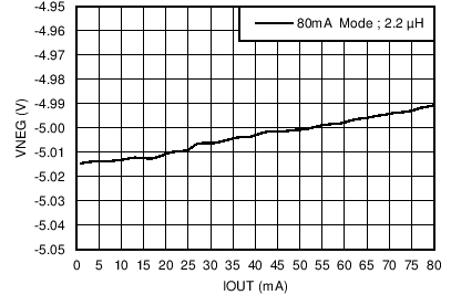
| VNEG = –5 V |
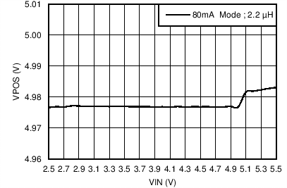
| VPOS = 5 V |
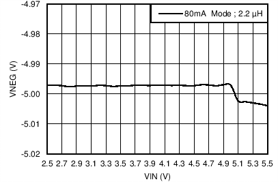
| VNEG = –5 V |

(with Active Discharge)

(with Active Discharge)

(TPS65132Ax only)
(TPS65132B2, –Lx, –Sx, –Wx)
| VPOS = 5.4 V |
| VNEG = –5.4 V |
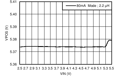
| VPOS = 5.4 V |
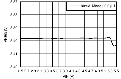
| VNEG = –5.4 V | |||
9.2.3 High-current Applications (≤ 150 mA)
The TPS65132Sx version allows output current up to 150 mA on both VPOS and VNEG when the SYNC pin is pulled HIGH. If the SYNC pin is pulled LOW, the TPS65132Sx can be programmed to 40mA or 80mA mode with the APPS bit to lower the output current capability of the VNEG rail if needed (in the case the efficiency is an important parameter). See Low-current Applications (≤ 40 mA) and Mid-current Applications (≤ 80 mA) for more details about the 40mA and 80mA modes.
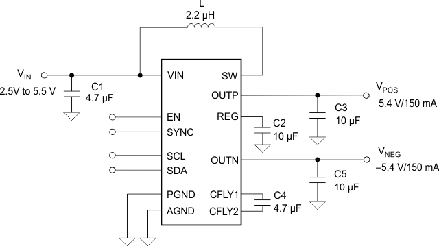 Figure 81. Typical Application Circuit For High Current
9.2.3.1 Design Requirements
Table 16. Design Parameters
| PARAMETERS | EXAMPLE VALUES |
|---|---|
| Input Voltage Range | 2.5 V to 5.5 V |
| Output Voltages | 4.0 V to 6.0 V, –4.0 V to –6.0 V |
| Output Current Rating | 150 mA |
| Boost Converter Switching Frequency | 1.8 MHz |
| Negative Charge Pump Switching Frequency | 1.0 MHz |
9.2.3.2 Detailed Design Procedure
The design procedure and BOM list of the TPS65132Sx is identical to the 80mA mode. Please refer to the Mid-current Applications (≤ 80 mA) for more details about the general component selection.
9.2.3.2.1 Sequencing
The output rails (VPOS and VNEG) are enabled and disabled using an external logic signal on the EN pin. The power-up and power-down sequencing events are programmable. Please refer to Programmable Sequencing Scenarios for the different sequencing as well as Registers for the programming options. Figure 98 to Figure 103 show the typical sequencing waveforms.
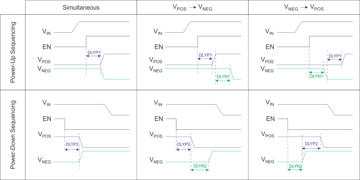 Figure 82. Programmable Sequencing Scenarios
NOTE
- In the case where the UVLO falling threshold is triggered while the enable signal is still HIGH (EN), all converters will be shut down instantaneously and both VPOS and VNEG output rails will be actively discharged to GND.
- The power-up and power-down sequencing must be finalized (all delays have passed) before re-toggling the EN pin.
9.2.3.2.2 SYNC = HIGH
When the SYNC pin is pulled HIGH, the boost converter voltage increases instantaneously to allow enough headroom to deliver the 150 mA. See Figure 88 to Figure 91 for detailed waveforms.
When SYNC pin is pulled LOW, the boost converter keeps its offset for 300 µs typically, and during this time, the device is still capable if supplying 150 mA on both output rail. After these 300 µs have passed, current limit settles at 40 mA or 80 mA maximum, depending on the application mode it is programmed to (40mA or 80mA — see Low-current Applications (≤ 40 mA) and Mid-current Applications (≤ 80 mA) for more details ) and the boost output voltage regulates down to its nominal value.
9.2.3.2.3 Startup
The TPS65132Sx can startup with SYNC = HIGH, however, the boost offset as well as the 150 mA output current capability will only be available as soon as the last rail to start is in regulation.
9.2.3.3 Application Curves
VIN= 3.7 V, VPOS= 5.4 V, VNEG= –5.4 V, unless otherwise notedTable 17. Component List For Typical Characteristics Circuits
| REFERENCE | DESCRIPTION | MANUFACTURER AND PART NUMBER |
|---|---|---|
| C | 2.2 µF, 16 V, 0603, X5R, ceramic | Murata - GRM188R61C225KAAD |
| 4.7 µF, 16 V, 0603, X5R, ceramic | Murata - GRM188R61C475KAAJ | |
| 10 μF, 16 V, 0603, X5R, ceramic | Murata - GRM188R61E106MA73 | |
| L | 2.2 µH, 2.4 A, 130 mΩ, 2.5 mm × 2.0 mm × 1.0 mm | Toko - DFE252010C (1269AS-H-2R2N=P2) |
| U1 | TPS65132SYFF | Texas Instruments |
Table 18. Table Of Graphs
| PARAMETER | CONDITIONS | Figure |
|---|---|---|
| EFFICIENCY | ||
| Efficiency vs. Output Current | ± 5.0 V — SYNC = HIGH — L = 2.2 µH | Figure 83 |
| Efficiency vs. Output Current | ± 5.4 V — SYNC = HIGH — L = 2.2 µH | Figure 84 |
| CONVERTERS WAVEFORMS | ||
| VPOS Output Ripple | IPOS = 150 mA — SYNC = HIGH | Figure 85 |
| VNEG Output Ripple | INEG = 10mA / 80 mA / 150 mA — SYNC = HIGH — COUT = 10 µF | Figure 86 |
| VNEG Output Ripple | INEG = 4 mA / 40 mA / 80 mA — SYNC = HIGH — COUT = 2 × 10 µF | Figure 87 |
| SYNC = HIGH Signal | ||
| SYNC = HIGH | IPOS = –INEG = 10 mA | Figure 88 |
| SYNC = HIGH | IPOS = –INEG = 150 mA | Figure 89 |
| SYNC = HIGH Zoom | IPOS = –INEG = 10 mA | Figure 90 |
| SYNC = LOW Zoom | IPOS = –INEG = 10 mA | Figure 91 |
| LOAD TRANSIENT | ||
| Load Transient | VIN = 2.9 V — IPOS = –INEG = 10 mA → 150 mA → 10 mA — SYNC = HIGH — L = 2.2 µH | Figure 92 |
| Load Transient | VIN = 3.7 V — IPOS = –INEG = 10 mA → 150 mA → 10 mA — SYNC = HIGH — L = 2.2 µH | Figure 93 |
| Load Transient | VIN = 4.5 V — IPOS = –INEG = 10 mA → 150 mA → 10mA — SYNC = HIGH — L = 2.2 µH | Figure 94 |
| LINE TRANSIENT | ||
| Line Transient | VIN = 2.8 V → 4.5 V → 2.8 V — IPOS = –INEG = 10 mA — SYNC = HIGH — L = 2.2 µH | Figure 95 |
| Line Transient | VIN = 2.8 V → 4.5 V → 2.8 V — IPOS = –INEG = 100 mA — SYNC = HIGH — L = 2.2 µH | Figure 96 |
| Line Transient | VIN = 2.8 V → 4.5 V → 2.8 V — IPOS = –INEG = 150 mA — SYNC = HIGH — L = 2.2 µH | Figure 97 |
| POWER SEQUENCING | ||
| Power-up Sequencing | Simultaneous — no load | Figure 98 |
| Power-down Sequencing | Simultaneous — no load with Active Discharge | Figure 99 |
| Power-up Sequencing | Sequential (VPOS → VNEG) — no load | Figure 100 |
| Power-down Sequencing | Sequential (VNEG → VPOS) — no load with Active Discharge | Figure 101 |
| Power-up Sequencing | Sequential (VNEG → VPOS) — no load | Figure 102 |
| Power-down Sequencing | Sequential (VPOS → VNEG) — no load with Active Discharge | Figure 103 |
| Power-up/down Sequencing | Simultaneous — no load without Active Discharge | Figure 104 |
| Power-up/down Sequencing | Simultaneous — no load with Active Discharge | Figure 105 |
| INRUSH CURRENT | ||
| Inrush Current | Simultaneous — no load — SYNC = HIGH — L = 2.2 µH | Figure 106 |
| Inrush Current | Sequential — no load — SYNC = HIGH — L = 2.2 µH | Figure 107 |
| LOAD REGULATION | ||
| VPOS vs Output Current | VPOS = 5.0 V — SYNC = HIGH — IPOS = 0 mA to 150 mA — L = 2.2 µH | Figure 108 |
| VPOS vs Output Current | VPOS = 5.4 V — SYNC = HIGH — IPOS = 0 mA to 150 mA — L = 2.2 µH | Figure 109 |
| VNEG vs Output Current | VNEG = –5.0 V — SYNC = HIGH — INEG = 0 mA to 150 mA — L = 2.2 µH | Figure 110 |
| VNEG vs Output Current | VNEG = –5.4 V — SYNC = HIGH — INEG = 0 mA to 150 mA — L = 2.2 µH | Figure 111 |
| LINE REGULATION | ||
| VPOS vs Output Voltage | VIN = 2.5 V to 5.5 V — VPOS = 5.0 V — SYNC = HIGH — IPOS = 120 mA — L = 2.2 µH | Figure 112 |
| VPOS vs Output Voltage | VIN = 2.5 V to 5.5 V — VPOS = 5.4 V — SYNC = HIGH — IPOS = 120 mA — L = 2.2 µH | Figure 113 |
| VNEG vs Output Voltage | VIN = 2.5 V to 5.5 V — VNEG = –5.0 V — SYNC = HIGH — INEG = 120 mA — L = 2.2 µH | Figure 114 |
| VNEG vs Output Voltage | VIN = 2.5 V to 5.5 V — VNEG = –5.4 V — SYNC = HIGH — INEG = 120 mA — L = 2.2 µH | Figure 115 |
spacer
NOTE
In this section, IOUT means that the outputs are loaded with IPOS = –INEG simultaneously.
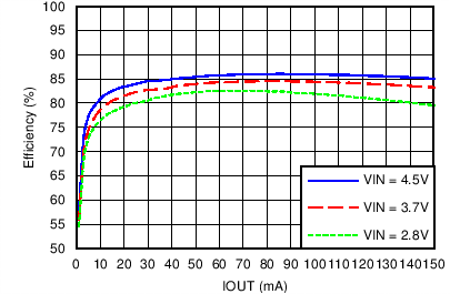 Figure 83. Combined Efficiency — ± 5.0 V — SYNC = HIGH
 L = 2.2 µH
 Figure 85. VPOS Output Voltage Ripple — SYNC = HIGH
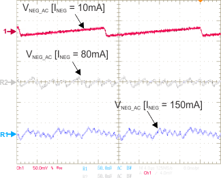 Figure 87. VNEG Output Voltage Ripple — SYNC = HIGH —
 L = 2.2 µH — COUT = 2 × 10 µF
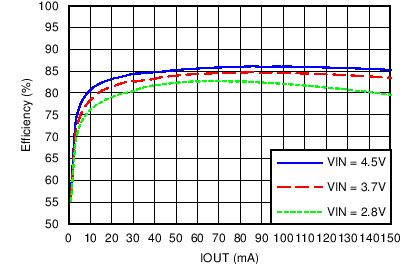 Figure 84. Combined Efficiency — ± 5.4 V — SYNC = HIGH
 L = 2.2 µH
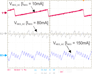 Figure 86. VNEG Output Voltage Ripple — SYNC = HIGH —
 L = 2.2 µH — COUT = 10 µF
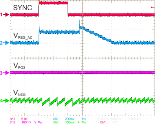 Figure 88. SYNC Signal — IOUT = 10 mA
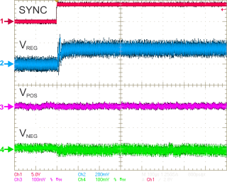 Figure 90. SYNC = HIGH (zoom)
 Figure 92. Load Transient — VIN = 2.9 V
SYNC = HIGH — ΔIOUT = 140 mA
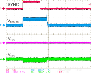 Figure 89. SYNC Signal — IOUT = 150 mA
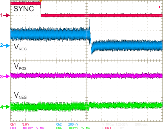 Figure 91. SYNC = LOW (zoom) with Delay
 Figure 93. Load Transient — VIN = 3.7 V
SYNC = HIGH — ΔIOUT = 140 mA
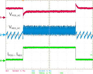 Figure 94. Load Transient — VIN = 4.5 V
SYNC = HIGH — ΔIOUT = 140 mA
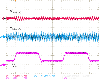 Figure 96. Line Transient — IOUT = 100 mA
SYNC = HIGH — ΔVIN = 1.7 V
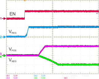 Figure 98. Power-Up Sequencing — Simultaneous
SYNC = HIGH
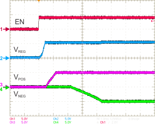 Figure 100. Power-Up Sequencing — Sequential
VPOS → VNEG — SYNC = HIGH
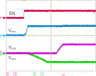 Figure 102. Power-Up Sequencing — Sequential
VNEG → VPOS — SYNC = HIGH
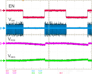 Figure 104. Power-Up/Down Without Active Discharge — SYNC = HIGH
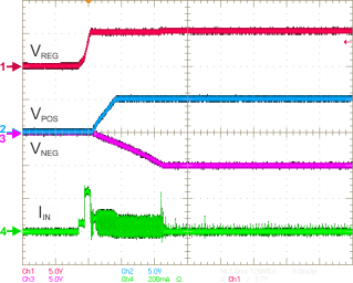 Figure 106. Inrush Current — Simultaneous —
 SYNC = HIGH
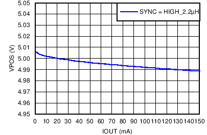 Figure 108. Load Regulation VPOS = 5.0 V — SYNC = HIGH
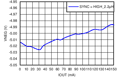 Figure 110. Load Regulation VNEG = –5.0 V — SYNC = HIGH
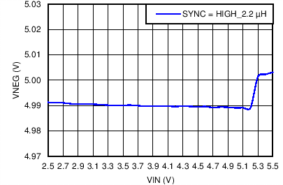 Figure 112. Line Regulation VPOS = 5.0 V — SYNC = HIGH
 Figure 114. Line Regulation VNEG = –5.0 V — SYNC = HIGH
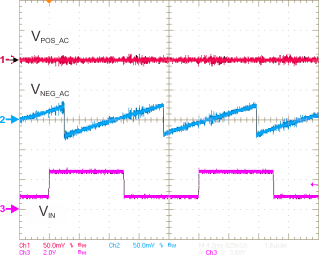 Figure 95. Line Transient — IOUT = 10 mA
SYNC = HIGH — ΔVIN = 1.7 V
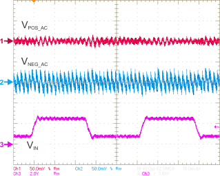 Figure 97. Line Transient — IOUT = 150 mA
 SYNC = HIGH — ΔVIN = 1.7 V
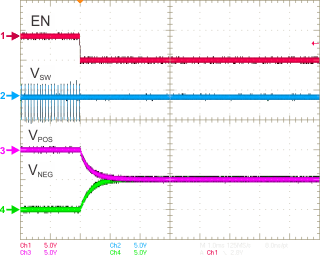 Figure 99. Power-Down Sequencing — Simultaneous
SYNC = HIGH
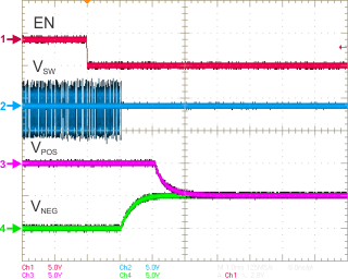 Figure 101. Power-Down Sequencing — Sequential
VNEG → VPOS— SYNC = HIGH
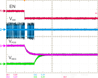 Figure 103. Power-Down Sequencing — Sequential
VPOS → VNEG — SYNC = HIGH
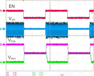 Figure 105. Power-Up/Down With Active Discharge — SYNC = HIGH
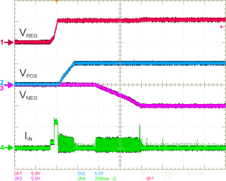 Figure 107. Inrush Current — Sequential
SYNC = HIGH
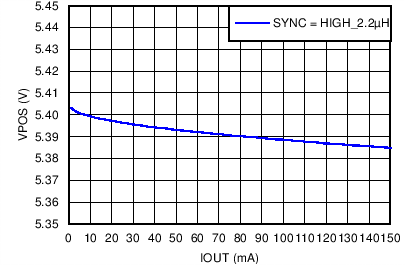 Figure 109. Load Regulation VPOS = 5.4 V — SYNC = HIGH
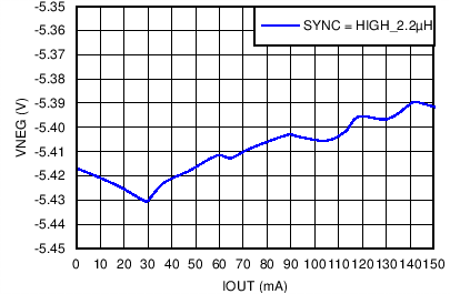 Figure 111. Load Regulation VNEG = –5.4 V — SYNC = HIGH
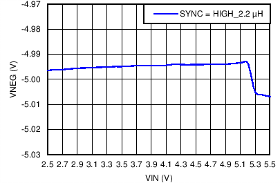 Figure 113. Line Regulation VPOS = 5.4 V — SYNC = HIGH
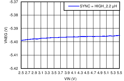 Figure 115. Line Regulation VNEG = –5.4 V — SYNC = HIGH