ZHCSCH4H June   2013  – November 2016 TPS65132 , TPS65132S

UNLESS OTHERWISE NOTED, this document contains PRODUCTION DATA.  

  1. 特性
  2. 应用范围
  3. 说明
  4. 修订历史记录
  5. Device Comparison Table
  6. Pin Configuration and Functions
  7. Specifications
    1. 7.1 Absolute Maximum Ratings
    2. 7.2 ESD Ratings
    3. 7.3 Recommended Operating Conditions
    4. 7.4 Thermal Information
    5. 7.5 Electrical Characteristics
    6. 7.6 I2C Interface Timing Requirements / Characteristics
    7. 7.7 Typical Characteristics
  8. Detailed Description
    1. 8.1 Overview
    2. 8.2 Functional Block Diagram
    3. 8.3 Feature Description
      1. 8.3.1 Undervoltage Lockout (UVLO)
      2. 8.3.2 Active Discharge
      3. 8.3.3 Boost Converter
        1. 8.3.3.1 Boost Converter Operation
        2. 8.3.3.2 Power-Up And Soft-Start (Boost Converter)
        3. 8.3.3.3 Power-Down (Boost Converter)
        4. 8.3.3.4 Isolation (Boost Converter)
        5. 8.3.3.5 Output Voltage (Boost Converter)
        6. 8.3.3.6 Advanced Power-Save Mode For Light-Load Efficiency And PFM
      4. 8.3.4 LDO Regulator
        1. 8.3.4.1 LDO Operation
        2. 8.3.4.2 Power-Up And Soft-Start (LDO)
        3. 8.3.4.3 Power-Down And Discharge (LDO)
        4. 8.3.4.4 Isolation (LDO)
        5. 8.3.4.5 Setting The Output Voltage (LDO)
      5. 8.3.5 Negative Charge Pump
        1. 8.3.5.1 Operation
        2. 8.3.5.2 Power-Up And Soft-Start (CPN)
        3. 8.3.5.3 Power-Down And Discharge (CPN)
        4. 8.3.5.4 Isolation (CPN)
        5. 8.3.5.5 Setting The Output Voltage (CPN)
    4. 8.4 Device Functional Modes
      1. 8.4.1 Enabling and Disabling the Device
    5. 8.5 Programming
      1. 8.5.1 I2C Serial Interface Description
      2. 8.5.2 I2C Interface Protocol
    6. 8.6 Register Maps
      1. 8.6.1 Registers
        1. 8.6.1.1 VPOS Register - Address: 0x00
        2. 8.6.1.2 VNEG Register - Address 0x01
        3. 8.6.1.3 DLYx Register - Address 0x02 (Only valid for TPS65132Sx)
        4. 8.6.1.4 APPS - SEQU - SEQD - DISP - DISN Register - Address 0x03
        5. 8.6.1.5 Control Register - Address 0xFF
      2. 8.6.2 Factory Default Register Value
  9. Application and Implementation
    1. 9.1 Application Information
    2. 9.2 Typical Applications
      1. 9.2.1 Low-current Applications (≤ 40 mA)
        1. 9.2.1.1 Design Requirements
        2. 9.2.1.2 Detailed Design Procedure
          1. 9.2.1.2.1 Sequencing
          2. 9.2.1.2.2 Boost Converter Design Procedure
            1. 9.2.1.2.2.1 Inductor Selection (Boost Converter)
            2. 9.2.1.2.2.2 Input Capacitor Selection (Boost Converter)
            3. 9.2.1.2.2.3 Output Capacitor Selection (Boost Converter)
          3. 9.2.1.2.3 Input Capacitor Selection (LDO)
          4. 9.2.1.2.4 Output Capacitor Selection (LDO)
          5. 9.2.1.2.5 Input Capacitor Selection (CPN)
          6. 9.2.1.2.6 Output Capacitor Selection (CPN)
          7. 9.2.1.2.7 Flying Capacitor Selection (CPN)
        3. 9.2.1.3 Application Curves
      2. 9.2.2 Mid-current Applications (≤ 80 mA)
        1. 9.2.2.1 Design Requirements
        2. 9.2.2.2 Detailed Design Procedure
          1. 9.2.2.2.1 Boost Converter Design Procedure
            1. 9.2.2.2.1.1 Inductor Selection (Boost Converter)
            2. 9.2.2.2.1.2 Input Capacitor Selection (Boost Converter)
            3. 9.2.2.2.1.3 Output Capacitor Selection (Boost Converter)
          2. 9.2.2.2.2 Input Capacitor Selection (LDO)
          3. 9.2.2.2.3 Output Capacitor Selection (LDO)
          4. 9.2.2.2.4 Input Capacitor Selection (CPN)
          5. 9.2.2.2.5 Output Capacitor Selection (CPN)
          6. 9.2.2.2.6 Flying Capacitor Selection (CPN)
        3. 9.2.2.3 Application Curves
      3. 9.2.3 High-current Applications (≤ 150 mA)
        1. 9.2.3.1 Design Requirements
        2. 9.2.3.2 Detailed Design Procedure
          1. 9.2.3.2.1 Sequencing
          2. 9.2.3.2.2 SYNC = HIGH
          3. 9.2.3.2.3 Startup
        3. 9.2.3.3 Application Curves
  10. 10Power Supply Recommendations
  11. 11Layout
    1. 11.1 Layout Guidelines
    2. 11.2 Layout Example
  12. 12器件和文档支持
    1. 12.1 器件支持
      1. 12.1.1 第三方米6体育平台手机版_好二三四免责声明
    2. 12.2 接收文档更新通知
    3. 12.3 社区资源
    4. 12.4 商标
    5. 12.5 静电放电警告
    6. 12.6 Glossary
  13. 13机械、封装和可订购信息
    1. 13.1 CSP 封装概要
      1. 13.1.1 芯片级封装尺寸
      2. 13.1.2 RVC 封装概要

Layout

Layout Guidelines

PCB layout is an important task in the power supply design. Good PCB layout minimizes EMI and allows very good output voltage regulation. For the TPS65132 the following PCB layout guidelines are recommended.

  • Keep the power ground plane on the top layer (all capacitor grounds and PGND pins must be connected together with one uninterrupted ground plane).
  • AGND and PGND must be connected together on the same ground plane.
  • Place the flying capacitor as close as possible to the IC.
  • Always avoid vias when possible. They have high inductance and resistance. If vias are necessary, always use more than one in parallel to decrease parasitics especially for power lines.
  • Connect REG pins together.
  • For high dv/dt signals (switch pin traces): keep copper area to a minimum to prevent making unintentional parallel plate capacitors with other traces or to a ground plane. Best to route signal and return on same layer.
  • For high di/dt signals: keep traces short, wide and closely spaced. This will reduce stray inductance and decrease the current loop area to help prevent EMI.
  • Keep input capacitor close to the IC with low inductance traces.
  • Keep trace from switching node pin to inductor short if possible: it reduces EMI emissions and noise that may couple into other portions of the converter.
  • Isolate analog signal paths from power paths.

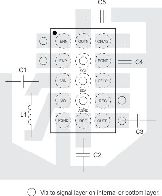
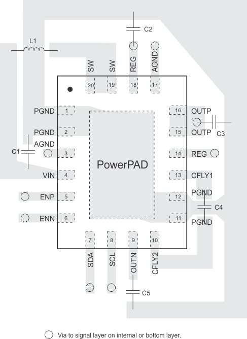
Layout Example

TPS65132 layout_slvsbm1.gif
Figure 116. PCB Layout Example for CSP Package
TPS65132 layout_QFN_slvsbm1.gif Figure 117. PCB Layout Example for QFN Package