ZHCSCH4H June   2013  – November 2016 TPS65132 , TPS65132S

UNLESS OTHERWISE NOTED, this document contains PRODUCTION DATA.  

  1. 特性
  2. 应用范围
  3. 说明
  4. 修订历史记录
  5. Device Comparison Table
  6. Pin Configuration and Functions
  7. Specifications
    1. 7.1 Absolute Maximum Ratings
    2. 7.2 ESD Ratings
    3. 7.3 Recommended Operating Conditions
    4. 7.4 Thermal Information
    5. 7.5 Electrical Characteristics
    6. 7.6 I2C Interface Timing Requirements / Characteristics
    7. 7.7 Typical Characteristics
  8. Detailed Description
    1. 8.1 Overview
    2. 8.2 Functional Block Diagram
    3. 8.3 Feature Description
      1. 8.3.1 Undervoltage Lockout (UVLO)
      2. 8.3.2 Active Discharge
      3. 8.3.3 Boost Converter
        1. 8.3.3.1 Boost Converter Operation
        2. 8.3.3.2 Power-Up And Soft-Start (Boost Converter)
        3. 8.3.3.3 Power-Down (Boost Converter)
        4. 8.3.3.4 Isolation (Boost Converter)
        5. 8.3.3.5 Output Voltage (Boost Converter)
        6. 8.3.3.6 Advanced Power-Save Mode For Light-Load Efficiency And PFM
      4. 8.3.4 LDO Regulator
        1. 8.3.4.1 LDO Operation
        2. 8.3.4.2 Power-Up And Soft-Start (LDO)
        3. 8.3.4.3 Power-Down And Discharge (LDO)
        4. 8.3.4.4 Isolation (LDO)
        5. 8.3.4.5 Setting The Output Voltage (LDO)
      5. 8.3.5 Negative Charge Pump
        1. 8.3.5.1 Operation
        2. 8.3.5.2 Power-Up And Soft-Start (CPN)
        3. 8.3.5.3 Power-Down And Discharge (CPN)
        4. 8.3.5.4 Isolation (CPN)
        5. 8.3.5.5 Setting The Output Voltage (CPN)
    4. 8.4 Device Functional Modes
      1. 8.4.1 Enabling and Disabling the Device
    5. 8.5 Programming
      1. 8.5.1 I2C Serial Interface Description
      2. 8.5.2 I2C Interface Protocol
    6. 8.6 Register Maps
      1. 8.6.1 Registers
        1. 8.6.1.1 VPOS Register - Address: 0x00
        2. 8.6.1.2 VNEG Register - Address 0x01
        3. 8.6.1.3 DLYx Register - Address 0x02 (Only valid for TPS65132Sx)
        4. 8.6.1.4 APPS - SEQU - SEQD - DISP - DISN Register - Address 0x03
        5. 8.6.1.5 Control Register - Address 0xFF
      2. 8.6.2 Factory Default Register Value
  9. Application and Implementation
    1. 9.1 Application Information
    2. 9.2 Typical Applications
      1. 9.2.1 Low-current Applications (≤ 40 mA)
        1. 9.2.1.1 Design Requirements
        2. 9.2.1.2 Detailed Design Procedure
          1. 9.2.1.2.1 Sequencing
          2. 9.2.1.2.2 Boost Converter Design Procedure
            1. 9.2.1.2.2.1 Inductor Selection (Boost Converter)
            2. 9.2.1.2.2.2 Input Capacitor Selection (Boost Converter)
            3. 9.2.1.2.2.3 Output Capacitor Selection (Boost Converter)
          3. 9.2.1.2.3 Input Capacitor Selection (LDO)
          4. 9.2.1.2.4 Output Capacitor Selection (LDO)
          5. 9.2.1.2.5 Input Capacitor Selection (CPN)
          6. 9.2.1.2.6 Output Capacitor Selection (CPN)
          7. 9.2.1.2.7 Flying Capacitor Selection (CPN)
        3. 9.2.1.3 Application Curves
      2. 9.2.2 Mid-current Applications (≤ 80 mA)
        1. 9.2.2.1 Design Requirements
        2. 9.2.2.2 Detailed Design Procedure
          1. 9.2.2.2.1 Boost Converter Design Procedure
            1. 9.2.2.2.1.1 Inductor Selection (Boost Converter)
            2. 9.2.2.2.1.2 Input Capacitor Selection (Boost Converter)
            3. 9.2.2.2.1.3 Output Capacitor Selection (Boost Converter)
          2. 9.2.2.2.2 Input Capacitor Selection (LDO)
          3. 9.2.2.2.3 Output Capacitor Selection (LDO)
          4. 9.2.2.2.4 Input Capacitor Selection (CPN)
          5. 9.2.2.2.5 Output Capacitor Selection (CPN)
          6. 9.2.2.2.6 Flying Capacitor Selection (CPN)
        3. 9.2.2.3 Application Curves
      3. 9.2.3 High-current Applications (≤ 150 mA)
        1. 9.2.3.1 Design Requirements
        2. 9.2.3.2 Detailed Design Procedure
          1. 9.2.3.2.1 Sequencing
          2. 9.2.3.2.2 SYNC = HIGH
          3. 9.2.3.2.3 Startup
        3. 9.2.3.3 Application Curves
  10. 10Power Supply Recommendations
  11. 11Layout
    1. 11.1 Layout Guidelines
    2. 11.2 Layout Example
  12. 12器件和文档支持
    1. 12.1 器件支持
      1. 12.1.1 第三方米6体育平台手机版_好二三四免责声明
    2. 12.2 接收文档更新通知
    3. 12.3 社区资源
    4. 12.4 商标
    5. 12.5 静电放电警告
    6. 12.6 Glossary
  13. 13机械、封装和可订购信息
    1. 13.1 CSP 封装概要
      1. 13.1.1 芯片级封装尺寸
      2. 13.1.2 RVC 封装概要

Pin Configuration and Functions

YFF Package
15 Bumps
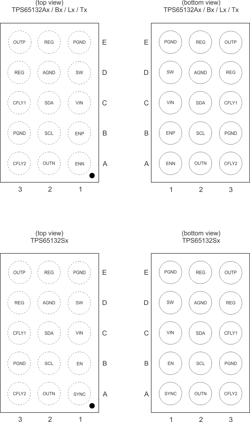
TPS65132 S_po_slvsbm1.gif

Pin Functions

PIN I/O DESCRIPTION
NAME Ax, Bx, Lx, Tx Sx
AGND D2 D2 Analog ground
CFLY1 C3 C3 I/O Negative charge pump flying capacitor pin
CFLY2 A3 A3 I/O Negative charge pump flying capacitor pin
EN B1 Enable pin (sequence programmed)
ENN A1 I Enable pin for VNEG rail
ENP B1 B1 I Enable pin for VPOS rail
OUTP E3 E3 O Output pin of the LDO (VPOS)
OUTN A2 A2 O Output pin of the negative charge pump (VNEG)
PGND B3 B3 Power ground
E1 E1
REG D3 D3 I/O Boost converter output pin
E2 E2
SCL B2 B2 I/O I²C interface clock signal pin
SDA C2 C2 I/O I²C interface data signal pin
SW D1 D1 I/O Switch pin of the boost converter
SYNC A1 I Synchronization pin. 150 mA current enabled if this pin is pulled HIGH.
VIN C1 C1 I Input voltage supply pin
QFN Package
20 Pins
TPS65132 QFN_po_slvsbm1.gif

Pin Functions

PIN I/O DESCRIPTION
NAME Wx
AGND 3 Analog ground
17
CFLY1 13 I/O Negative charge pump flying capacitor pin
CFLY2 10 I/O Negative charge pump flying capacitor pin
ENN 6 I Enable pin for VNEG rail
ENP 5 I Enable pin for VPOS rail
OUTP 16 O Output pin of the LDO (VPOS)
15
OUTN 9 O Output pin of the negative charge pump (VNEG)
PGND 1 Power ground
2
11
12
REG 14 I/O Boost converter output pin
18
SCL 8 I/O I²C interface clock signal pin
SDA 7 I/O I²C interface data signal pin
SW 19 I/O Switch pin of the boost converter
20
VIN 4 I Input voltage supply pin