ZHCSCM6G May 2014 – October 2019 SN65HVD70 , SN65HVD71 , SN65HVD73 , SN65HVD74 , SN65HVD76 , SN65HVD77
PRODUCTION DATA.
- 1 特性
- 2 应用
- 3 说明
- 4 修订历史记录
- 5 Device Comparison Table
- 6 Pin Configuration and Functions
-
7 Specifications
- 7.1 Absolute Maximum Ratings
- 7.2 ESD Ratings
- 7.3 Recommended Operating Conditions
- 7.4 Thermal Information — D Packages
- 7.5 Thermal Information — DGS and DGK Packages
- 7.6 Power Dissipation
- 7.7 Electrical Characteristics
- 7.8 Switching Characteristics — 400 kbps
- 7.9 Switching Characteristics — 20 Mbps
- 7.10 Switching Characteristics — 50 Mbps
- 7.11 Typical Characteristics
- 8 Parameter Measurement Information
- 9 Detailed Description
- 10Application and Implementation
- 11Power Supply Recommendations
- 12Layout
- 13器件和文档支持
- 14机械、封装和可订购信息
10.2.1.4 Receiver Failsafe
The differential receivers of the SN65HVD7x family are failsafe to invalid bus states caused by the following:
- Open bus conditions, such as a disconnected connector
- Shorted bus conditions, such as cable damage shorting the twisted-pair together
- Idle bus conditions that occur when no driver on the bus is actively driving
In any of these cases, the differential receiver will output a failsafe logic high state so that the output of the receiver is not indeterminate.
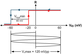
Receiver failsafe is accomplished by offsetting the receiver thresholds such that the input indeterminate range does not include zero volts differential. In order to comply with the RS-422 and RS-485 standards, the receiver output must output a high when the differential input VID is more positive than 200 mV, and must output a Low when VID is more negative than –200 mV. The receiver parameters which determine the failsafe performance are VIT+, VIT–, and Vhys (the separation between VIT+ and VIT–). As shown in the Electrical Characteristics table, differential signals more negative than –200 mV will always cause a low receiver output, and differential signals more positive than 200 mV will always cause a high receiver output.
When the differential input signal is close to zero, it is still above the VIT+ threshold, and the receiver output will be High. Only when the differential input is more than Vhys below VIT+ will the receiver output transition to a Low state. Therefore, the noise immunity of the receiver inputs during a bus fault conditions includes the receiver hysteresis value, Vhys, as well as the value of VIT+.
 Figure 33. SN65HVD7x Noise Immunity Under Bus Fault Conditions