ZHCSCV2C june   2014  – may 2023 TPS65263

PRODUCTION DATA  

  1.   1
  2. 特性
  3. 应用
  4. 说明
  5. Revision History
  6. Device Comparison Table
  7. Pin Configuration and Functions
  8. Specifications
    1. 7.1 Absolute Maximum Ratings
    2. 7.2 ESD Ratings
    3. 7.3 Recommended Operating Conditions
    4. 7.4 Thermal Information
    5. 7.5 Electrical Characteristics
    6. 7.6 Typical Characteristics
  9. Detailed Description
    1. 8.1 Overview
    2. 8.2 Functional Block Diagram
    3. 8.3 Feature Description
      1. 8.3.1  Adjusting the Output Voltage
      2. 8.3.2  Enable and Adjusting UVLO
      3. 8.3.3  Soft-Start Time
      4. 8.3.4  Power-Up Sequencing
      5. 8.3.5  V7V Low Dropout Regulator and Bootstrap
      6. 8.3.6  Out-of-Phase Operation
      7. 8.3.7  Output Overvoltage Protection (OVP)
      8. 8.3.8  Pulse Skipping Mode (PSM)
      9. 8.3.9  Slope Compensation
      10. 8.3.10 Overcurrent Protection
        1. 8.3.10.1 High-Side MOSFET Overcurrent Protection
        2. 8.3.10.2 Low-Side MOSFET Overcurrent Protection
      11. 8.3.11 Power Good
      12. 8.3.12 Thermal Shutdown
    4. 8.4 Device Functional Modes
      1. 8.4.1 Serial Interface Description
      2. 8.4.2 I2C Update Sequence
    5. 8.5 Register Maps
      1. 8.5.1 Register Description
      2. 8.5.2 VOUT1_SEL: Vout1 Voltage Selection Register (offset = 0x00H)
      3. 8.5.3 VOUT2_SEL: Vout2 Voltage Selection Register (offset = 0x01H)
      4. 8.5.4 VOUT3_SEL: Vout3 Voltage Selection Register (offset = 0x02H)
      5. 8.5.5 VOUT1_COM: Buck1 Command Register (offset = 0x03H)
      6. 8.5.6 VOUT2_COM: Buck2 Command Register (offset = 0x04H)
      7. 8.5.7 VOUT3_COM: Buck3 Command Register (offset = 0x05H)
      8. 8.5.8 SYS_STATUS: System Status Register (offset = 0x06H)
  10. Application and Implementation
    1. 9.1 Application Information
    2. 9.2 Typical Application
      1. 9.2.1 Design Requirements
      2. 9.2.2 Detailed Design Procedure
        1. 9.2.2.1 Output Inductor Selection
        2. 9.2.2.2 Output Capacitor Selection
        3. 9.2.2.3 Input Capacitor Selection
        4. 9.2.2.4 Loop Compensation
      3. 9.2.3 Application Curves
    3. 9.3 Power Supply Recommendations
    4. 9.4 Layout
      1. 9.4.1 Layout Guidelines
      2. 9.4.2 Layout Example
  11. 10Device and Documentation Support
    1. 10.1 接收文档更新通知
    2. 10.2 支持资源
    3. 10.3 Trademarks
    4. 10.4 静电放电警告
    5. 10.5 术语表
  12. 11Mechanical, Packaging, and Orderable Information

Typical Characteristics

TA = 25°C, VIN = 12 V, VOUT1= 1.5 V, VOUT2= 1.2 V, VOUT3= 2.5 V, FSW = 600 kHz (unless otherwise noted)
GUID-1AC241BF-255A-4B51-B6D7-907A8109BA17-low.png
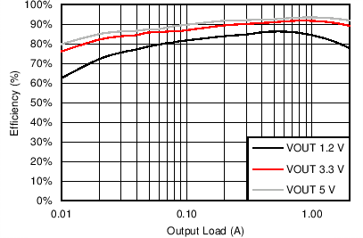
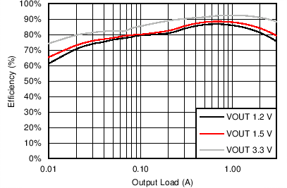
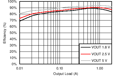
Figure 7-1 BUCK1 Efficiency
GUID-2CF63F24-7613-42A9-8B4C-581C54FA6704-low.png
Figure 7-3 BUCK3 Efficiency
GUID-9F8ABB4A-9B2C-4499-BE18-FDBF72243DC5-low.png
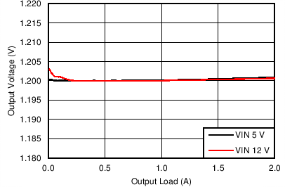
Figure 7-5 BUCK2 Load Regulation
GUID-599C17ED-3A18-47EF-8746-B116DC0999B3-low.png
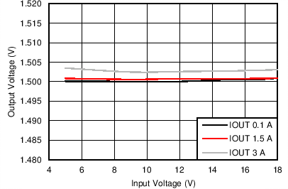
Figure 7-7 BUCK1, Line Regulation
GUID-49623203-421C-4079-9907-18DF6E03E754-low.png
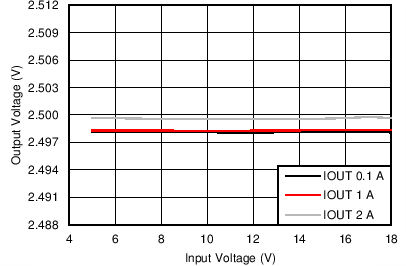
Figure 7-9 BUCK3, Line Regulation
GUID-33619B29-6CA6-4A5D-B150-F602B456AC9F-low.png
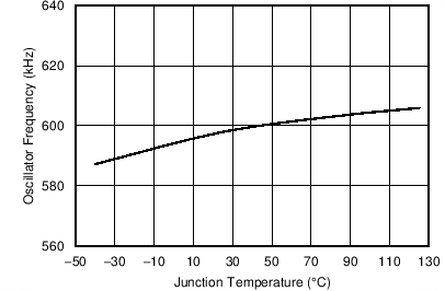
Figure 7-11 Oscillator Reference vs Temperature
GUID-4F6E0C61-F24C-4531-930D-64B6158B923D-low.png
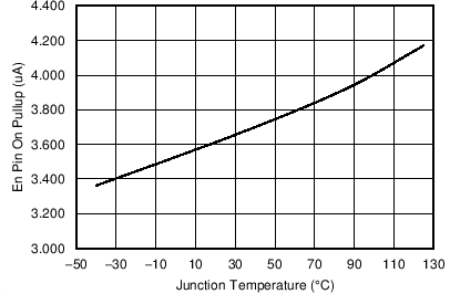
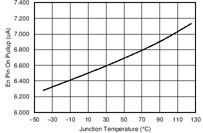
Figure 7-13 EN Pin Pullup Current vs Temperature, EN = 1 V
GUID-6F9480F3-7DC6-4A4A-B67A-480ED76B9212-low.png
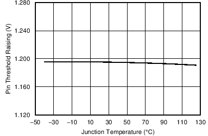
Figure 7-15 EN Pin Threshold Rising vs Temperature
GUID-AA32E6C7-8A2E-495E-A733-66F7EE3F7A5B-low.png
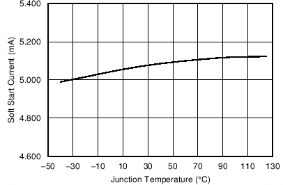
Figure 7-17 SS Pin Charge Current vs Temperature
GUID-41C04784-A624-413C-AEEC-FAFBBFB4C754-low.png
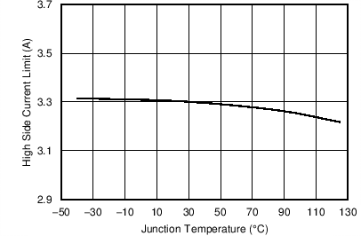
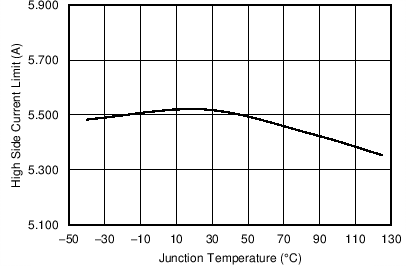
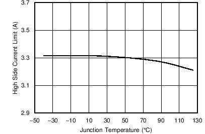
Figure 7-19 Buck2 High-Side Current Limit vs Temperature
GUID-AB08834C-24D5-445B-A6E0-8B639A6E740F-low.png
Figure 7-2 BUCK2 Efficiency
GUID-69D7F809-18E5-4CB5-9707-53A7F697A4AA-low.png
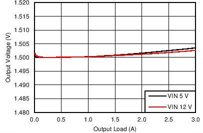
Figure 7-4 BUCK1 Load Regulation
GUID-0DA8BAAE-5852-423A-B4B1-A2BCD31A2A9F-low.png
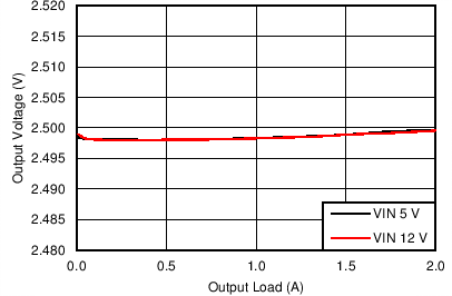
Figure 7-6 BUCK3 Load Regulation
GUID-4DA9DDE7-FBE5-4B95-B3A9-19C85A407034-low.png
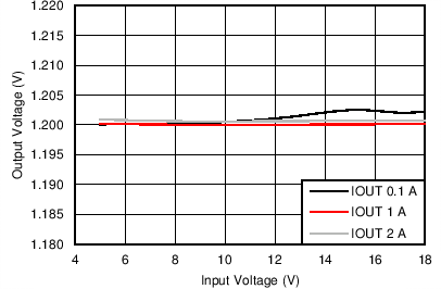
Figure 7-8 BUCK2, Line Regulation
GUID-F2ED61E6-D860-4070-ADA3-13A35A68A8A4-low.png
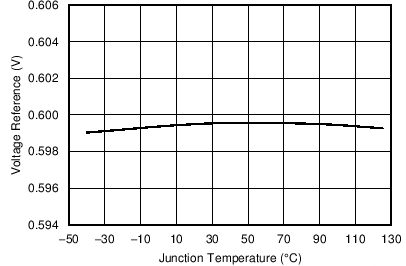
Figure 7-10 Voltage Reference vs Temperature
GUID-20C040F1-EFB9-48AD-8CF1-3343F7008603-low.png
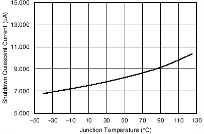
Figure 7-12 Shurtdown Quiescent Current vs Temperature
GUID-2B858F4B-CA5D-4028-A5E7-134E776999E4-low.png
Figure 7-14 EN Pin Pullup Current vs Temperature, EN = 1.5 V
GUID-EAC86222-5679-4C81-83B2-8C1FD734296B-low.png
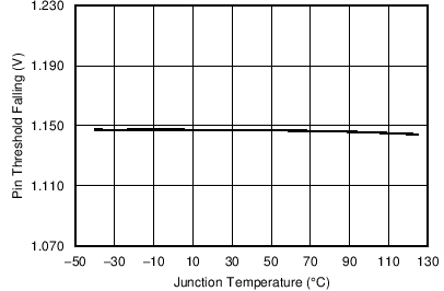
Figure 7-16 EN Pin Threshold Falling vs Temperature
GUID-41086EF2-E0EB-4E2B-B178-CD7966242E6D-low.png
Figure 7-18 Buck1 High-Side Current Limit vs Temperature
GUID-DCCB4313-7922-4EFA-AFA0-8A2CD8698439-low.png
Figure 7-20 Buck3 High-Side Current Limit vs Temperature