ZHCSCZ0F June 2014 – March 2017 AMC1305L25 , AMC1305M05 , AMC1305M25
PRODUCTION DATA.
- 1 特性
- 2 应用
- 3 说明
- 4 修订历史记录
- 5 Device Comparison Table
- 6 Pin Configuration and Functions
-
7 Specifications
- 7.1 Absolute Maximum Ratings
- 7.2 ESD Ratings
- 7.3 Recommended Operating Conditions
- 7.4 Thermal Information
- 7.5 Power Ratings
- 7.6 Insulation Specifications
- 7.7 Safety-Related Certifications
- 7.8 Safety Limiting Values
- 7.9 Electrical Characteristics: AMC1305M05
- 7.10 Electrical Characteristics: AMC1305x25
- 7.11 Switching Characteristics
- 7.12 Insulation Characteristics Curves
- 7.13 Typical Characteristics
- 8 Detailed Description
- 9 Application and Implementation
- 10Power-Supply Recommendations
- 11Layout
- 12器件和文档支持
- 13机械、封装和可订购信息
9 Application and Implementation
NOTE
Information in the following applications sections is not part of the TI component specification, and TI does not warrant its accuracy or completeness. TI’s customers are responsible for determining suitability of components for their purposes. Customers should validate and test their design implementation to confirm system functionality.
9.1 Application Information
9.1.1 Digital Filter Usage
The modulator generates a bit stream that is processed by a digital filter to obtain a digital word similar to a conversion result of a conventional analog-to-digital converter (ADC). A very simple filter, built with minimal effort and hardware, is a sinc3-type filter, as shown in Equation 2:

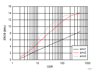
This filter provides the best output performance at the lowest hardware size (count of digital gates) for a second-order modulator. All the characterization in this document is also done with a sinc3 filter with an over-sampling ratio (OSR) of 256 and an output word width of 16 bits.

An example code for an implementation of a sinc3 filter in an FPGA, see the application note Combining ADS1202 with FPGA Digital Filter for Current Measurement in Motor Control Applications (SBAA094), available for download at www.ti.com.
9.2 Typical Applications
9.2.1 Frequency Inverter Application
Because to their high ac and dc performance, isolated ΔΣ modulators are being widely used in new generation frequency inverter designs. Frequency inverters are critical parts of industrial motor drives, photovoltaic inverters (string and central inverters), uninterruptible power supplies (UPS), electrical and hybrid electrical vehicles, and other industrial applications. The input structure of the AMC1305 is optimized for use with low-impedance shunt resistors and is therefore tailored for isolated current sensing using shunts.
9.2.1.1 Design Requirements
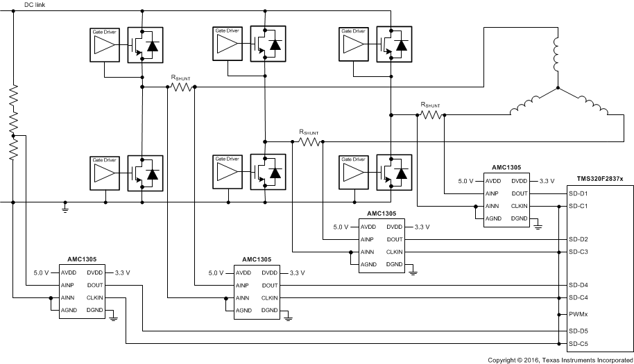
A typical operation of the device in a frequency inverter application is shown in Figure 54. When the inverter stage is part of a motor drive system, measurement of the motor phase current is done via the shunt resistors (RSHUNT). Depending on the system design, either all three or only two phase currents are sensed.
In this example, an additional fourth AMC1305 is used to support isolated voltage sensing of the dc link. This high voltage is reduced using a high-impedance resistive divider before being sensed by the device across a smaller resistor. The value of this resistor can degrade the performance of the measurement, as described in the Isolated Voltage Sensing section.
9.2.1.2 Detailed Design Procedure
The usually recommended RC filter in front of a ΔΣ modulator to improve signal-to-noise performance of the signal path, is not required for the AMC1305. By design, the input bandwidth of the analog front-end of the device is limited to 1 MHz.
For modulator output bit-stream filtering, a device from TI's TMS320F2837x family of dual-core MCUs is recommended. This family supports up to eight channels of dedicated hardwired filter structures that significantly simplify system level design by offering two filtering paths per channel: one providing high accuracy results for the control loop and one fast response path for overcurrent detection.
9.2.1.3 Application Curve
In motor control applications, a very fast response time for overcurrent detection is required. The time for fully settling the filter in case of a step-signal at the input of the modulator depends on its order; that is, a sinc3 filter requires three data updates for full settling (with fDATA = fCLK / OSR). Therefore, for overcurrent protection, filter types other than sinc3 can be a better choice; an alternative is the sinc2 filter. Figure 55 compares the settling times of different filter orders.
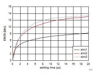
The delay time of the sinc filter with a continuous signal is half of its settling time.
9.2.2 Isolated Voltage Sensing
The AMC1305 is optimized for usage in current-sensing applications using low-impedance shunts. However, the device can also be used in isolated voltage-sensing applications if the impact of the (usually higher) impedance of the resistor used in this case is considered.
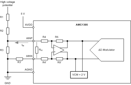 Figure 56. Using AMC1305 for Isolated Voltage Sensing
9.2.2.1 Design Requirements
Figure 56 shows a simplified circuit typically used in high-voltage sensing applications. The high impedance resistors (R1 and R2) are used as voltage dividers and dominate the current value definition. The resistance of the sensing resistor R3 is chosen to meet the input voltage range of the AMC1305. This resistor and the differential input impedance of the device (the AMC1305x25 is 25 kΩ, the AMC1305M05 is 5 kΩ) also create a voltage divider that results in an additional gain error. With the assumption of R1, R2, and RIN having a considerably higher value than R3, the resulting total gain error can be estimated using Equation 4, with EG being the gain error of the AMC1305.

This gain error can be easily minimized during the initial system level gain calibration procedure.
9.2.2.2 Detailed Design Procedure
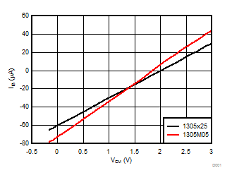
As indicated in Figure 56, the output of the integrated differential amplifier is internally biased to a common-mode voltage of 2 V. This voltage results in a bias current IIB through the resistive network R4 and R5 (or R4' and R5') used for setting the gain of the amplifier. The value range of this current is specified in the Electrical Characteristics table. This bias current generates additional offset error that depends on the value of the resistor R3. Because the value of this bias current depends on the actual common-mode amplitude of the input signal (as shown in Figure 57), the initial system offset calibration does not minimize its effect. Therefore, in systems with high accuracy requirements TI recommends using a series resistor at the negative input (AINN) of the AMC1305 with a value equal to the shunt resistor R3 (that is R3' = R3 in Figure 56) to eliminate the effect of the bias current.
This additional series resistor (R3') influences the gain error of the circuit. The effect can be calculated using Equation 5 with R5 = R5' = 50 kΩ and R4 = R4' = 2.5 kΩ (for the AMC1305M05) or 12.5 kΩ (for the AMC1305x25).

9.2.2.3 Application Curve
Figure 57 shows the dependency of the input bias current on the common-mode voltage at the input of the AMC1305.
