ZHCSD00C June   2014  – December 2015 ADS7042

PRODUCTION DATA.  

  1. 特性
  2. 应用
  3. 说明
  4. 修订历史记录
  5. Pin Configuration and Functions
  6. Specifications
    1. 6.1 Absolute Maximum Ratings
    2. 6.2 ESD Ratings
    3. 6.3 Recommended Operating Conditions
    4. 6.4 Thermal Information
    5. 6.5 Electrical Characteristics
    6. 6.6 Timing Characteristics
    7. 6.7 Typical Characteristics
  7. Parameter Measurement Information
    1. 7.1 Digital Voltage Levels
  8. Detailed Description
    1. 8.1 Overview
    2. 8.2 Functional Block Diagram
    3. 8.3 Feature Description
      1. 8.3.1 Reference
      2. 8.3.2 Analog Input
      3. 8.3.3 ADC Transfer Function
      4. 8.3.4 Serial Interface
    4. 8.4 Device Functional Modes
      1. 8.4.1 Offset Calibration
        1. 8.4.1.1 Offset Calibration on Power-Up
        2. 8.4.1.2 Offset Calibration During Normal Operation
  9. Application and Implementation
    1. 9.1 Application Information
    2. 9.2 Typical Applications
      1. 9.2.1 Single-Supply DAQ with the ADS7042
        1. 9.2.1.1 Design Requirements
        2. 9.2.1.2 Detailed Design Procedure
          1. 9.2.1.2.1 Antialiasing Filter
          2. 9.2.1.2.2 Input Amplifier Selection
          3. 9.2.1.2.3 Reference Circuit
        3. 9.2.1.3 Application Curve
      2. 9.2.2 DAQ Circuit with the ADS7042 for Maximum SINAD
        1. 9.2.2.1 Design Requirements
        2. 9.2.2.2 Detailed Design Procedure
        3. 9.2.2.3 Application Curves
      3. 9.2.3 12-Bit, 10-kSPS DAQ Circuit Optimized for DC Sensor Measurements
        1. 9.2.3.1 Design Requirements
        2. 9.2.3.2 Detailed Design Procedure
        3. 9.2.3.3 Application Curve
  10. 10Power-Supply Recommendations
    1. 10.1 AVDD and DVDD Supply Recommendations
    2. 10.2 Estimating Digital Power Consumption
    3. 10.3 Optimizing Power Consumed by the Device
  11. 11Layout
    1. 11.1 Layout Guidelines
    2. 11.2 Layout Example
  12. 12器件和文档支持
    1. 12.1 文档支持
      1. 12.1.1 相关文档 
    2. 12.2 社区资源
    3. 12.3 商标
    4. 12.4 静电放电警告
    5. 12.5 Glossary
  13. 13机械、封装和可订购信息

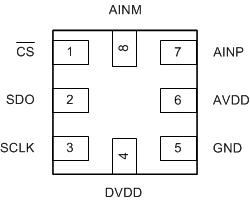
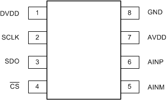
5 Pin Configuration and Functions

RUG Package
8-Pin X2QFN
Top View
ADS7042 po_rug8_bas608.gif
DCU Package
8-Pin Leaded VSSOP
Top View
ADS7042 po_dcu8_bas608.gif

Pin Functions

PIN I/O DESCRIPTION
NAME NO.
RUG DCU
AINM 8 5 Analog input Analog signal input, negative
AINP 7 6 Analog input Analog signal input, positive
AVDD 6 7 Supply Analog power-supply input, also provides the reference voltage to the ADC
CS 1 4 Digital input Chip-select signal, active low
DVDD 4 1 Supply Digital I/O supply voltage
GND 5 8 Supply Ground for power supply, all analog and digital signals are referred to this pin
SCLK 3 2 Digital input Serial clock
SDO 2 3 Digital output Serial data out