ZHCSDA1D July 2012 – August 2017 DS90UB926Q-Q1
PRODUCTION DATA.
- 1 特性
- 2 应用范围
- 3 说明
- 4 修订历史记录
- 5 说明 (续)
- 6 Pin Configuration and Functions
-
7 Specifications
- 7.1 Absolute Maximum Ratings
- 7.2 ESD Ratings
- 7.3 Recommended Operating Conditions
- 7.4 Thermal Information
- 7.5 DC Electrical Characteristics
- 7.6 AC Electrical Characteristics
- 7.7 DC and AC Serial Control Bus Characteristics
- 7.8 Timing Requirements
- 7.9 Timing Requirements for the Serial Control Bus
- 7.10 Switching Characteristics
- 7.11 Timing Diagrams
- 7.12 Typical Characteristics
-
8 Detailed Description
- 8.1 Overview
- 8.2 Functional Block Diagram
- 8.3
Feature Description
- 8.3.1 High-Speed Forward Channel Data Transfer
- 8.3.2 Low-Speed Back Channel Data Transfer
- 8.3.3 Backward-Compatible Mode
- 8.3.4 Input Equalization Gain
- 8.3.5 Common-Mode Filter Pin (CMF)
- 8.3.6 Video Control Signal Filter
- 8.3.7 EMI Reduction Features
- 8.3.8 Enhanced Progressive Turnon (EPTO)
- 8.3.9 LVCMOS VDDIO Option
- 8.3.10 Power Down (PDB)
- 8.3.11 Stop Stream Sleep
- 8.3.12 Serial Link Fault Detect
- 8.3.13 Oscillator Output
- 8.3.14 Pixel Clock Edge Select (RFB)
- 8.3.15 Image Enhancement Features
- 8.3.16 Internal Pattern Generation
- 8.3.17 Built-In Self Test (BIST)
- 8.3.18 I2S Receiving
- 8.3.19 Interrupt Pin — Functional Description and Usage (INTB)
- 8.3.20 GPIO[3:0] and GPO_REG[8:4]
- 8.4 Device Functional Modes
- 8.5 Programming
- 8.6 Register Maps
- 9 Application and Implementation
- 10Power Supply Recommendations
- 11Layout
- 12器件和文档支持
- 13机械、封装和可订购信息
10 Power Supply Recommendations
10.1 Power Up Requirements and PDB Pin
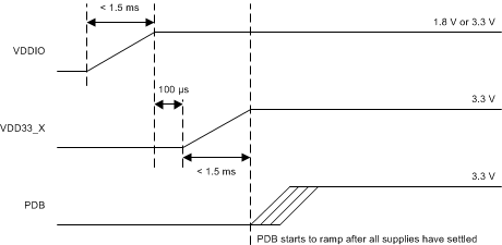
When VDDIO and VDD33_X are powered separately, the VDDIO supply (1.8 V or 3.3 V) must ramp 100 µs before the other supply (VDD33_X) begins to ramp. If VDDIO is tied with VDD33_X, both supplies may ramp at the same time. The VDDs (VDD33_X and VDDIO) supply ramp must be faster than 1.5 ms with a monotonic rise. A large capacitor on the PDB pin is required to ensure PDB arrives after all the VDDs have settled to the recommended operating voltage. When PDB pin is pulled to VDDIO = 3 V to 3.6 V or VDD33_X, TI recommends using a 10-kΩ pullup and a > 10-µF capacitor to GND to delay the PDB input signal.
All inputs must not be driven until VDD33_X and VDDIO has reached its steady-state value.
 Figure 28. Power-Up Sequence of DS90UB926Q-Q1