ZHCSDA1D July 2012 – August 2017 DS90UB926Q-Q1
PRODUCTION DATA.
- 1 特性
- 2 应用范围
- 3 说明
- 4 修订历史记录
- 5 说明 (续)
- 6 Pin Configuration and Functions
-
7 Specifications
- 7.1 Absolute Maximum Ratings
- 7.2 ESD Ratings
- 7.3 Recommended Operating Conditions
- 7.4 Thermal Information
- 7.5 DC Electrical Characteristics
- 7.6 AC Electrical Characteristics
- 7.7 DC and AC Serial Control Bus Characteristics
- 7.8 Timing Requirements
- 7.9 Timing Requirements for the Serial Control Bus
- 7.10 Switching Characteristics
- 7.11 Timing Diagrams
- 7.12 Typical Characteristics
-
8 Detailed Description
- 8.1 Overview
- 8.2 Functional Block Diagram
- 8.3
Feature Description
- 8.3.1 High-Speed Forward Channel Data Transfer
- 8.3.2 Low-Speed Back Channel Data Transfer
- 8.3.3 Backward-Compatible Mode
- 8.3.4 Input Equalization Gain
- 8.3.5 Common-Mode Filter Pin (CMF)
- 8.3.6 Video Control Signal Filter
- 8.3.7 EMI Reduction Features
- 8.3.8 Enhanced Progressive Turnon (EPTO)
- 8.3.9 LVCMOS VDDIO Option
- 8.3.10 Power Down (PDB)
- 8.3.11 Stop Stream Sleep
- 8.3.12 Serial Link Fault Detect
- 8.3.13 Oscillator Output
- 8.3.14 Pixel Clock Edge Select (RFB)
- 8.3.15 Image Enhancement Features
- 8.3.16 Internal Pattern Generation
- 8.3.17 Built-In Self Test (BIST)
- 8.3.18 I2S Receiving
- 8.3.19 Interrupt Pin — Functional Description and Usage (INTB)
- 8.3.20 GPIO[3:0] and GPO_REG[8:4]
- 8.4 Device Functional Modes
- 8.5 Programming
- 8.6 Register Maps
- 9 Application and Implementation
- 10Power Supply Recommendations
- 11Layout
- 12器件和文档支持
- 13机械、封装和可订购信息
8 Detailed Description
8.1 Overview
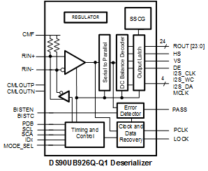
The DS90UB926Q-Q1 deserializer receives 35 bits of data over a single serial FPD-Link III pair operating up to 2.975-Gbps application payload. The serial stream contains an embedded clock, video control signals, and the DC-balanced video data and audio data which enhance signal quality to support AC coupling.
The DS90UB926Q-Q1 deserializer attains lock to a data stream without the use of a separate reference clock source, which greatly simplifies system complexity and overall cost. The deserializer also synchronizes to the serializer regardless of the data pattern, delivering true automatic plug and lock performance. It can lock to the incoming serial stream without the need of special training patterns or sync characters. The deserializer recovers the clock and data by extracting the embedded clock information, validating then deserializing the incoming data stream. The recovered parallel LVCMOS video bus is then provided to the display. The deserializer is intended for use with the DS90UB925Q-Q1 serializer, but is also backward-compatible with DS90UR905Q or DS90UR907Q FPD-Link II serializer.
8.2 Functional Block Diagram
8.3 Feature Description
8.3.1 High-Speed Forward Channel Data Transfer
The High-Speed Forward Channel (HS_FC) is composed of 35 bits of data containing DIN[23:0] or RGB[7:0] or YUV data, sync signals, I2C, and I2S audio transmitted from Serializer to Deserializer. Figure 12 shows the serial stream per PCLK cycle. This data payload is optimized for signal transmission over an AC-coupled link. Data is randomized, balanced, and scrambled.
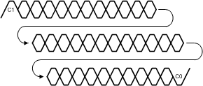 Figure 12. FPD-Link III Serial Stream
The device supports clocks in the range of 5 MHz to 85 MHz. The application payload rate is 2.975 Gbps maximum (175 Mbps minimum) with the actual line rate of 2.975 Gbps maximum and 525 Mbps minimum.
8.3.2 Low-Speed Back Channel Data Transfer
The low-speed backward channel (LS_BC) of the DS90UB926Q-Q1 provides bidirectional communication between the display and host processor. The information is carried back from the Deserializer to the Serializer per serial symbol. The back channel control data is transferred over the single serial link along with the high-speed forward data, DC balance coding and embedded clock information. This architecture provides a backward path across the serial link together with a high-speed forward channel. The back channel contains the I2C, CRC, and 4 bits of standard GPIO information with 10-Mbps line rate.
8.3.3 Backward-Compatible Mode
The DS90UB926Q-Q1 is also backward-compatible to DS90UR905Q and DS90UR907Q FPD Link II serializers at 15- to 65-MHz pixel clock frequencies. It receives 28 bits of data over a single serial FPD-Link II pair operating at the line rate of 420 Mbps to 1.82 Gbps. This backward-compatible mode is provided through the MODE_SEL pin (Table 9) or the configuration register (Table 11). In this mode, the minimum PCLK frequency is 15 MHz.
8.3.4 Input Equalization Gain
FPD-Link III input adaptive equalizer provides compensation for transmission medium losses and reduces the medium-induced deterministic jitter. It equalizes up to 10 meter STP cables with 3 connection breaks at maximum serialized stream payload rate of 2.975 Gbps.
8.3.5 Common-Mode Filter Pin (CMF)
The deserializer provides access to the center tap of the internal termination. A capacitor must be placed on this pin for additional common-mode filtering of the differential pair. This can be useful in high noise environments for additional noise rejection capability. A 0.1-μF capacitor has to be connected to this pin to Ground.
8.3.6 Video Control Signal Filter
When operating the devices in Normal Mode, the Video Control Signals (DE, HS, VS) have the following restrictions:
- Normal Mode with Control Signal Filter Enabled: DE and HS — Only 2 transitions per 130 clock cycles are transmitted, the transition pulse must be 3 PCLK or longer.
- Normal Mode with Control Signal Filter Disabled: DE and HS — Only 2 transitions per 130 clock cycles are transmitted, no restriction on minimum transition pulse.
- VS — Only 1 transition per 130 clock cycles are transmitted, minimum pulse width is 130 clock cycles.
Video Control Signals are defined as low frequency signals with limited transitions. Glitches of a control signal can cause a visual display error. This feature allows for the chipset to validate and filter out any high-frequency noise on the control signals. See Figure 13.
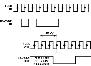 Figure 13. Video Control Signal Filter Waveform
8.3.7 EMI Reduction Features
8.3.7.1 Spread Spectrum Clock Generation (SSCG)
The DS90UB926Q-Q1 provides an internally generated spread-spectrum clock (SSCG) to modulate its outputs. Both clock and data outputs are modulated. This will aid to lower system EMI. Output SSCG deviations to ±2.5% (5% total) at up to 100-kHz modulations are available. This feature may be controlled by register. See Table 1, Table 2, and Table 11. Do not enable the SSCG feature if the source PCLK into the SER has a clock with spread spectrum already.
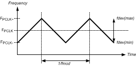 Figure 14. SSCG Waveform
Table 1. SSCG Configuration
LFMODE = L (15 to 85 MHz)
| SSCG CONFIGURATION (0x2C) LFMODE = L (15 to 85 MHz) | SPREAD SPECTRUM OUTPUT | |||
|---|---|---|---|---|
| SSC[2] | SSC[1] | SSC[0] | Fdev (%) | Fmod (kHz) |
| L | L | L | ±0.9 | PCLK / 2168 |
| L | L | H | ±1.2 | |
| L | H | L | ±1.9 | |
| L | H | H | ±2.5 | |
| H | L | L | ±0.7 | PCLK / 1300 |
| H | L | H | ±1.3 | |
| H | H | L | ±2 | |
| H | H | H | ±2.5 | |
Table 2. SSCG Configuration
LFMODE = H (5 to <15 MHz)
| SSCG CONFIGURATION (0x2C) LFMODE = H (5 to <15 MHz) | SPREAD SPECTRUM OUTPUT | |||
|---|---|---|---|---|
| SSC[2] | SSC[1] | SSC[0] | Fdev (%) | Fmod (kHz) |
| L | L | L | ±0.5 | PCLK / 628 |
| L | L | H | ±1.3 | |
| L | H | L | ±1.8 | |
| L | H | H | ±2.5 | |
| H | L | L | ±0.7 | PCLK / 388 |
| H | L | H | ±1.2 | |
| H | H | L | ±2 | |
| H | H | H | ±2.5 | |
8.3.8 Enhanced Progressive Turnon (EPTO)
The deserializer LVCMOS parallel outputs timing are delayed. Groups of 8-bit R, G and B outputs switch in a different time. This minimizes the number of outputs switching simultaneously and helps to reduce supply noise. In addition, it spreads the noise spectrum out reducing overall EMI.
8.3.9 LVCMOS VDDIO Option
The deserializer parallel bus can operate with 1.8-V or 3.3-V levels (VDDIO) for target (display) compatibility. The 1.8-V levels offers a lower noise (EMI) and also a system power savings.
8.3.10 Power Down (PDB)
The Serializer has a PDB input pin to ENABLE or POWER DOWN the device. This pin can be controlled by the host or through the VDDIO, where VDDIO = 3 V to 3.6 V or VDD33. To save power disable the link when the display is not needed (PDB = LOW). When the pin is driven by the host, make sure to release it after VDD33 and VDDIO have reached final levels; no external components are required. In the case of driven by the VDDIO = 3 V to 3.6 V or VDD33 directly, a 10-kΩ resistor to the VDDIO = 3 V to 3.6 V or VDD33 , and a > 10-µF capacitor to the ground are required (see Figure 24).
8.3.11 Stop Stream Sleep
The deserializer enters a low power SLEEP state when the input serial stream is stopped. A STOP condition is detected when the embedded clock bits are not present. When the serial stream starts again, the deserializer then locks to the incoming signal and recover the data.
NOTE
In STOP STREAM SLEEP, the Serial Control Bus Registers values are retained.
8.3.12 Serial Link Fault Detect
The serial link fault detection is able to detect any of following 7 conditions
- cable open
- + to – short
- + short to GND
- - short to GND
- + short to battery
- - short to battery
- cable is linked incorrectly
If any one of the fault conditions occurs, The Link Detect Status is 0 (cable is not detected) on the Serial Control Bus Register bit 0 of address 0x1C Table 11. The link errors can be monitored though Link Error Count of the Serial Control Bus Register bit [4:0] of address 0x41 Table 11.
8.3.13 Oscillator Output
The deserializer provides an optional PCLK output when the input clock (serial stream) has been lost. This is based on an internal oscillator. The frequency of the oscillator may be selected. This feature is controlled by register Address 0x02, bit 5 (OSC Clock Enable). See Table 11.
8.3.14 Pixel Clock Edge Select (RFB)
The RFB determines the edge that the data is strobed on. If RFB is High (1), output data is strobed on the Rising edge of the PCLK. If RFB is Low (‘0’), data is strobed on the Falling edge of the PCLK. This allows for inter-operability with downstream devices. The deserializer output does not need to use the same edge as the Ser input. This feature may be controlled by register. See Table 11.
8.3.15 Image Enhancement Features
Several image enhancement features are provided. White balance LUTs allow the user to define and target the color temperature of the display. Adaptive Hi-FRC dithering enables the presentation of “true-color” images on an 18–bit color display.
8.3.15.1 White Balance
The white balance feature enables similar display appearance when using LCDs from different vendors. It compensates for native color temperature of the display, and adjusts relative intensities of R, G, and B to maintain specified color temperature. Programmable control registers are used to define the contents of three LUTs (8-bit color value for red, green and blue) for the white balance feature. The LUTs map input RGB values to new output RGB values. There are three LUTs, one LUT for each color. Each LUT contains 256 entries, 8 bits per entry with a total size of 6144 bits (3 x 256 x 8). All entries are readable and writable. Calibrated values are loaded into registers through the I2C interface (deserializer is a slave device). This feature may also be applied to lower color depth applications such as 18-bit (666) and 16-bit (565). White balance is enabled and configured through the serial control bus register.
8.3.15.1.1 LUT Contents
The user must define and load the contents of the LUT for each color (R,G, and B). Regardless of the color depth being driven (888, 666, 656), the user must always provide contents for 3 complete LUTs - 256 colors × 8 bits × 3 tables. Unused bits - LSBs -shall be set to 0 by the user.
When 24-bit (888) input data is being driven to a 24-bit display, each LUT (R, G and B) must contain 256 unique 8-bit entries. The 8-bit white balanced data is then available at the output of the DS90UB926Q-Q1 deserializer, and driven to the display.
When 18-bit (666) input data is being driven to an 18-bit display, the white balance feature may be used in one of two ways. First, simply load each LUT with 256, 8-bit entries. Each 8-bit entry is a 6-bit value (6 MSBs) with the 2 LSBs set to 00. Thus as total of 64 unique 6-bit white balance output values are available for each color (R, G, and B). The 6-bit white balanced data is available at the output of the DS90UB926Q-Q1 deserializer, and driven directly to the display.
Alternatively, with 6-bit input data the user may choose to load complete 8-bit values into each LUT. This mode of operation provides the user with finer resolution at the LUT output to more closely achieve the desired white point of the calibrated display. Although 8-bit data is loaded, only 64 unique 8-bit white balance output values are available for each color (R, G, and B). The result is 8-bit white balanced data. Before driving to the output of the deserializer, the 8-bit data must be reduced to 6-bit with an FRC dithering function. To operate in this mode, the user must configure the DS90UB926Q-Q1 to enable the FRC2 function.
Examples of the three types of LUT configurations described are shown in Figure 15
8.3.15.1.2 Enabling White Balance
The user must load all 3 LUTs prior to enabling the white balance feature. The following sequence must be followed by the user.
To initialize white balance after power-on (Table 3):
- Load contents of all 3 LUTs . This requires a sequential loading of LUTs - first RED, second GREEN, third BLUE. 256, 8-bit entries must be loaded to each LUT. Page registers must be set to select each LUT.
- Enable white balance
By default, the LUT data may not be reloaded after initialization at power-on.
An option does exist to allow LUT reloading after power-on and initial LUT loading (as described above). This option may only be used after enabling the white balance reload feature through the associated serial control bus register. In this mode the LUTs may be reloaded by the master controller through the I2C. This provides the user with the flexibility to refresh LUTs periodically , or upon system requirements to change to a new set of LUT values. The host controller loads the updated LUT values through the serial bus interface. There is no need to disable the white balance feature while reloading the LUT data. Refreshing the white balance to the new set of LUT data will be seamless - no interruption of displayed data.
It is important to note that initial loading of LUT values requires that all 3 LUTs be loaded sequentially. When reloading, partial LUT updates may be made.
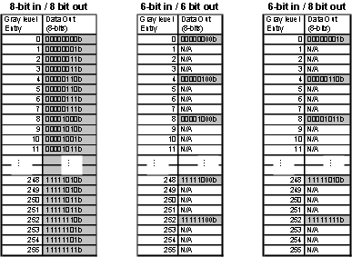 Figure 15. White Balance LUT Configurations
Table 3. White Balance Register Table
| PAGE | ADD (dec) | ADD (hex) | REGISTER NAME | BIT(s) | ACCESS | DEFAULT (hex) | FUNCTION | DESCRIPTION |
|---|---|---|---|---|---|---|---|---|
| 0 | 42 | 0x2A | White Balance Control | 7:6 | RW | 0x00 | Page Setting | 00: Configuration Registers 01: Red LUT 10: Green LUT 11: Blue LUT |
| 5 | RW | White Balance Enable | 0: White Balance Disable 1: White Balance Enable |
|||||
| 4 | RW | 0: Reload Disable 1: Reload Enable |
||||||
| 3:0 | Reserved | |||||||
| 1 | 0 – 255 | 00 – FF | White Balance Red LUT | FF:0 | RW | N/A | Red LUT | 256 8–bit entries to be applied to the Red subpixel data |
| 2 | 0 – 255 | 00 – FF | White Balance Green LUT | FF:0 | RW | N/A | Green LUT | 256 8–bit entries to be applied to the Green subpixel data |
| 3 | 0 – 255 | 00 – FF | White Balance Blue LUT | FF:0 | RW | N/A | Blue LUT | 256 8–bit entries to be applied to the Blue subpixel data |
8.3.15.2 Adaptive HI-FRC Dithering
The adaptive FRC dithering feature delivers product-differentiating image quality. It reduces 24-bit RGB (8 bits per subpixel) to 18-bit RGB (6 bits per sub-pixel), smoothing color gradients, and allowing the flexibility to use lower cost 18-bit displays. Frame Rate Control (FRC) dithering is a method to emulate “missing” colors on a lower color depth LCD display by changing the pixel color slightly with every frame. FRC is achieved by controlling on and off pixels over multiple frames (Temporal). Static dithering regulates the number of on and off pixels in a small defined pixel group (Spatial). The FRC module includes both Temporal and Spatial methods and also Hi-FRC. Conventional FRC can display only 16,194,277 colors with 6-bit RGB source. “Hi-FRC” enables full (16,777,216) color on an 18-bit LCD panel. The “adaptive” FRC module also includes input pixel detection to apply specific Spatial dithering methods for smoother gray level transitions. When enabled, the lower LSBs of each RGB output are not active; only 18-bit data (6 bits per R,G and B) are driven to the display. This feature is enabled through the serial control bus register.
Two FRC functional blocks are available, and may be independently enabled. FRC1 precedes the white balance LUT, and is intended to be used when 24-bit data is being driven to an 18-bit display with a white balance LUT that is calibrated for an 18-bit data source. The second FRC block, FRC2, follows the white balance block and is intended to be used when fine adjustment of color temperature is required on an 18-bit color display, or when a 24-bit source drives an 18-bit display with a white balance LUT calibrated for 24-bit source data.
For proper operation of the FRC dithering feature, the user must provide a description of the display timing control signals. The timing mode, “sync mode” (HS, VS) or “DE only” must be specified, along with the active polarity of the timing control signals. All this information is entered to DS90UB926Q-Q1 control registers through the serial bus interface.
Adaptive Hi-FRC dithering consists of several components. Initially, the incoming 8-bit data is expanded to 9-bit data. This allows the effective dithered result to support a total of 16.7 million colors. The incoming 9-bit data is evaluated, and one of four possible algorithms is selected. The majority of incoming data sequences are supported by the default dithering algorithm. Certain incoming data patterns (black/white pixel, full on/off sub-pixel) require special algorithms designed to eliminate visual artifacts associated with these specific gray level transitions. Three algorithms are defined to support these critical transitions.
An example of the default dithering algorithm is illustrated in Figure 16. The 1 or 0 value shown in the table describes whether the 6-bit value is increased by 1 (1) or left unchanged (0). In this case, the 3 truncated LSBs are 001.
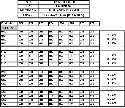 Figure 16. Default FRC Algorithm
See Table 4 for recommended FRC settings dependant on 18/24–bit source, 18/24–bit white balance LUT, and 18/24–bit display.
Table 4. Recommended FRC settings
| SOURCE | WHITE BALANCE LUT | DISPLAY | FRC1 | FRC2 |
|---|---|---|---|---|
| 24–bit | 24–bit | 24–bit | Disabled | Disabled |
| 24–bit | 24–bit | 18–bit | Disabled | Enabled |
| 24–bit | 18–bit | 18–bit | Enabled | Disabled |
| 18–bit | 24–bit | 24–bit | Disabled | Disabled |
| 18–bit | 24–bit | 18–bit | Disabled | Enabled |
| 18–bit | 18–bit | 18–bit | Disabled | Disabled |
8.3.16 Internal Pattern Generation
The DS90UB926Q-Q1 serializer supports the internal pattern generation feature. It allows basic testing and debugging of an integrated panel. The test patterns are simple and repetitive and allow for a quick visual verification of panel operation. As long as the device is not in power-down mode, the test pattern will be displayed even if no parallel input is applied. If no PCLK is received, the test pattern can be configured to use a programmed oscillator frequency. For detailed information, refer to AN-2198 Exploring the Internal Test Pattern Generation Feature of 720p FPD-Link III Devices (SNLA132).
8.3.17 Built-In Self Test (BIST)
An optional at-speed built-in self test (BIST) feature supports the testing of the high speed serial link and the low-speed back channel. This is useful in the prototype stage, equipment production, in-system test, and also for system diagnostics.
NOTE
BIST is not available in backward-compatible mode.
8.3.17.1 BIST Configuration and Status
The BIST mode is enabled at the deserializer by the pin select (Pin 44 BISTEN and Pin 16 BISTC) or configuration register (Table 11) through the deserializer. When LFMODE = 0, the pin-based configuration defaults to external PCLK or 33-MHz internal oscillator clock (OSC) frequency. In the absence of PCLK, the user can select the desired OSC frequency (default 33 MHz or 25 MHz) through the register bit. When LFMODE = 1, the pin based configuration defaults to external PCLK or 12.5MHz MHz internal oscillator clock (OSC) frequency.
When BISTEN of the deserializer is high, the BIST mode enable information is sent to the serializer through the Back Channel. The serializer outputs a test pattern and drives the link at speed. The deserializer detects the test pattern and monitors it for errors. The PASS output pin toggles to flag any payloads that are received with 1 to 35 bit errors.
The BIST status is monitored real time on PASS pin. The result of the test is held on the PASS output until reset (new BIST test or Power Down). A high on PASS indicates NO ERRORS were detected. A Low on PASS indicates one or more errors were detected. The duration of the test is controlled by the pulse width applied to the deserializer BISTEN pin. This BIST feature also contains a Link Error Count and a Lock Status. If the connection of the serial link is broken, then the link error count is shown in the register. When the PLL of the deserializer is locked or unlocked, the lock status can be read in the register. See Table 11.
8.3.17.1.1 Sample BIST Sequence
See Figure 17 for the BIST mode flow diagram.
- For the DS90UB925Q-Q1 and DS90UB926Q-Q1 FPD-Link III chipset, BIST Mode is enabled through the BISTEN pin of DS90UB926Q-Q1 FPD-Link III deserializer. The desired clock source is selected through BISTC pin.
- The DS90UB925Q-Q1 serializer is woken up through the back channel if it is not already on. The all zero pattern on the data pins is sent through the FPD-Link III to the deserializer. Once the serializer and the deserializer are in BIST mode and the deserializer acquires Lock, the PASS pin of the deserializer goes high and BIST starts checking the data stream. If an error in the payload (1 to 35) is detected, the PASS pin will switch low for one half of the clock period. During the BIST test, the PASS output can be monitored and counted to determine the payload error rate.
- To Stop the BIST mode, the deserializer BISTEN pin is set Low. The deserializer stops checking the data. The final test result is held on the PASS pin. If the test ran error free, the PASS output will be High. If there was one or more errors detected, the PASS output will be Low. The PASS output state is held until a new BIST is run, the device is RESET, or Powered Down. The BIST duration is user controlled by the duration of the BISTEN signal.
- The Link returns to normal operation after the deserializer BISTEN pin is low. Figure 18 shows the waveform diagram of a typical BIST test for two cases. Case 1 is error free, and Case 2 shows one with multiple errors. In most cases it is difficult to generate errors due to the robustness of the link (differential data transmission etc.), thus they may be introduced by greatly extending the cable length, faulting the interconnect, reducing signal condition enhancements ( Rx Equalization).
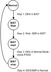 Figure 17. BIST Mode Flow Diagram
8.3.17.2 Forward Channel And Back Channel Error Checking
While in BIST mode, the serializer stops sampling RGB input pins and switches over to an internal all-zero pattern. The internal all-zeroes pattern goes through scrambler, DC-balancing, and so forth, and goes over the serial link to the deserializer. The deserializer on locking to the serial stream compares the recovered serial stream with all-zeroes and records any errors in status registers and dynamically indicates the status on PASS pin. The deserializer then outputs a SSO pattern on the RGB output pins.
The back-channel data is checked for CRC errors once the serializer locks onto back-channel serial stream as indicated by link detect status (register bit 0x0C[0]). The CRC errors are recorded in an 8-bit register. The register is cleared when the serializer enters the BIST mode. As soon as the serializer exits BIST mode, the functional mode CRC register starts recording the CRC errors. The BIST mode CRC error register is active in BIST mode only and keeps the record of last BIST run until cleared or enters BIST mode again.
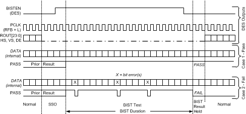 Figure 18. Bist Waveforms
8.3.18 I2S Receiving
In normal 24-bit RGB operation mode, the DS90UB926Q-Q1 provides up to 3-bit of I2S. They are I2S_CLK, I2S_WC and I2S_DA, as well as the Master I2S Clock (MCLK). The audio is received through the forward video frame, or can be configured to receive during video blanking periods. A jitter cleaning feature reduces I2S_CLK output jitter to +/- 2ns.
8.3.18.1 I2S Jitter Cleaning
The DS90UB926Q-Q1 features a standalone PLL to clean the I2S data jitter supporting high end car audio systems. If I2S CLK frequency is less than 1MHz, this feature has to be disabled through the register bit I2S Control (0x2B) in Table 10
8.3.18.2 Secondary I2S Channel
In 18-bit RGB operation mode, the secondary I2S data (I2S_DB) can be used as the additional I2S audio channel in additional to the 3–bit of I2S. The I2S_DB is synchronized to the I2S_CLK. To enable this synchronization feature on this bit, set the MODE_SEL (Table 9) or program through the register bit (Table 11).
8.3.18.2.1 MCLK
The deserializer has an I2S Master Clock Output. It supports x1, x2, or x4 of I2S CLK Frequency. When the I2S PLL is disabled, the MCLK output is off. Table 5 below covers the range of I2S sample rates and MCLK frequencies. By default, all the MCLK output frequencies are x2 of the I2S CLK frequencies. The MCLK frequencies can also be enabled through the register bit [7:4] (I2S MCLK Output) of 0x3A shown in Table 11. To select desired MCLK frequency, write bit 7 (0x3A) = 1, then write to bit [6:4] accordingly.
Table 5. Audio Interface Frequencies
| SAMPLE RATE (kHz) |
I2S DATA WORD SIZE (BITS) |
I2S CLK (MHz) |
MCLK OUTPUT (MHz) |
REGISTER 0x3A[6:4]'b |
|---|---|---|---|---|
| 32 | 16 | 1.024 | I2S_CLK x1 | 000 |
| I2S_CLK x2 | 001 | |||
| I2S_CLK x4 | 010 | |||
| 44.1 | 1.4112 | I2S_CLK x1 | 000 | |
| I2S_CLK x2 | 001 | |||
| I2S_CLK x4 | 010 | |||
| 48 | 1.536 | I2S_CLK x1 | 000 | |
| I2S_CLK x2 | 001 | |||
| I2S_CLK x4 | 010 | |||
| 96 | 3.072 | I2S_CLK x1 | 001 | |
| I2S_CLK x2 | 010 | |||
| I2S_CLK x4 | 011 | |||
| 192 | 6.144 | I2S_CLK x1 | 010 | |
| I2S_CLK x2 | 011 | |||
| I2S_CLK x4 | 100 | |||
| 32 | 24 | 1.536 | I2S_CLK x1 | 000 |
| I2S_CLK x2 | 001 | |||
| I2S_CLK x4 | 010 | |||
| 44.1 | 2.117 | I2S_CLK x1 | 001 | |
| I2S_CLK x2 | 010 | |||
| I2S_CLK x4 | 011 | |||
| 48 | 2.304 | I2S_CLK x1 | 001 | |
| I2S_CLK x2 | 010 | |||
| I2S_CLK x4 | 011 | |||
| 96 | 4.608 | I2S_CLK x1 | 010 | |
| I2S_CLK x2 | 011 | |||
| I2S_CLK x4 | 100 | |||
| 192 | 9.216 | I2S_CLK x1 | 011 | |
| I2S_CLK x2 | 100 | |||
| I2S_CLK x4 | 101 | |||
| 32 | 32 | 2.048 | I2S_CLK x1 | 001 |
| I2S_CLK x2 | 010 | |||
| I2S_CLK x4 | 011 | |||
| 44.1 | 2.8224 | I2S_CLK x1 | 001 | |
| I2S_CLK x2 | 010 | |||
| I2S_CLK x4 | 011 | |||
| 48 | 3.072 | I2S_CLK x1 | 001 | |
| I2S_CLK x2 | 010 | |||
| I2S_CLK x4 | 011 | |||
| 96 | 6.144 | I2S_CLK x1 | 010 | |
| I2S_CLK x2 | 011 | |||
| I2S_CLK x4 | 100 | |||
| 192 | 12.288 | I2S_CLK x1 | 011 | |
| I2S_CLK x2 | 100 | |||
| I2S_CLK x4 | 110 |
8.3.19 Interrupt Pin — Functional Description and Usage (INTB)
- On DS90UB925Q-Q1, set register 0xC6[5] = 1 and 0xC6[0] = 1
- DS90UB926Q-Q1 deserializer INTB_IN (pin 16) is set LOW by some downstream device.
- DS90UB925Q-Q1 serializer pulls INTB (pin 31) LOW. The signal is active low, so a LOW indicates an interrupt condition.
- External controller detects INTB = LOW; to determine interrupt source, read ISR register .
- A read to ISR will clear the interrupt at the DS90UB925Q-Q1, releasing INTB.
- The external controller typically must then access the remote device to determine downstream interrupt source and clear the interrupt driving INTB_IN. This would be when the downstream device releases the INTB_IN (pin 16) on the DS90UB926Q-Q1. The system is now ready to return to step (1) at next falling edge of INTB_IN.
8.3.20 GPIO[3:0] and GPO_REG[8:4]
In 18-bit RGB operation mode, the optional R[1:0] and G[1:0] of the DS90UB926Q-Q1 can be used as the general purpose IOs GPIO[3:0] in either forward channel (Outputs) or back channel (Inputs) application.
GPIO[3:0] Enable Sequence
See Table 6 for the GPIO enable sequencing.
- Enable the 18-bit mode either through the configuration register bit Table 11 on DS90UB925Q-Q1 only. DS90UB926Q-Q1 is automatically configured as in the 18-bit mode.
- To enable GPIO3 forward channel, write 0x03 to address 0x0F on DS90UB925Q-Q1, then write 0x05 to address 0x1F on DS90UB926Q-Q1.
Table 6. GPIO Enable Sequencing Table
| NO. | DESCRIPTION | DEVICE | FORWARD CHANNEL | BACK CHANNEL |
|---|---|---|---|---|
| 1 | Enable 18-bit mode | DS90UB925Q-Q1 | 0x12 = 0x04 | 0x12 = 0x04 |
| DS90UB926Q-Q1 | Auto Load from DS90UB925Q-Q1 | Auto Load from DS90UB925Q-Q1 | ||
| 2 | GPIO3 | DS90UB925Q-Q1 | 0x0F = 0x03 | 0x0F = 0x05 |
| DS90UB926Q-Q1 | 0x1F = 0x05 | 0x1F = 0x03 | ||
| 3 | GPIO2 | DS90UB925Q-Q1 | 0x0E = 0x30 | 0x0E = 0x50 |
| DS90UB926Q-Q1 | 0x1E = 0x50 | 0x1E = 0x30 | ||
| 4 | GPIO1 | DS90UB925Q-Q1 | 0x0E = 0x03 | 0x0E = 0x05 |
| DS90UB926Q-Q1 | 0x1E = 0x05 | 0x0E = 0x05 | ||
| 5 | GPIO0 | DS90UB925Q-Q1 | 0x0D = 0x93 | 0x0D = 0x95 |
| DS90UB926Q-Q1 | 0x1D = 0x95 | 0x1D = 0x93 |
8.3.20.1 GPO_REG[8:4] Enable Sequence
GPO_REG[8:4] are the outputs only pins. They must be programmed through the local register bits. See Table 7 for the GPO_REG enable sequencing.
- Enable the 18-bit mode either through the configuration register bit Table 11 on DS90UB925Q-Q1 only. DS90UB926Q-Q1 is automatically configured as in the 18-bit mode.
- To enable GPO_REG8 outputs a 1 , write 0x90 to address 0x21 on DS90UB926Q-Q1.
Table 7. GPO_REG Enable Sequencing Table
| NO. | DESCRIPTION | DEVICE | LOCAL ACCESS | LOCAL OUTPUT VALUE |
|---|---|---|---|---|
| 1 | Enable 18-bit mode | DS90UB926Q-Q1 | 0x12 = 0x04 (on DS90UB925Q-Q1) |
|
| 2 | GPO_REG8 | DS90UB926Q-Q1 | 0x21 = 0x90 | 1 |
| 0x21 = 0x10 | 0 | |||
| 3 | GPO_REG7 | DS90UB926Q-Q1 | 0x21 = 0x09 | 1 |
| 0x21 = 0x01 | 1 | |||
| 4 | GPO_REG6 | DS90UB926Q-Q1 | 0x20 = 0x90 | 0 |
| 0x20 = 0x10 | 1 | |||
| 5 | GPO_REG5 | DS90UB926Q-Q1 | 0x20 = 0x09 | 1 |
| 0x20 = 0x01 | 0 | |||
| 6 | GPO_REG4 | DS90UB926Q-Q1 | 0x1F = 0x90 | 1 |
| 0x1F = 0x10 | 0 |
8.4 Device Functional Modes
8.4.1 Clock-Data Recovery Status Flag (LOCK), Output Enable (OEN) and Output State Select (OSS_SEL)
When PDB is driven HIGH, the CDR PLL begins locking to the serial input and LOCK is TRI-STATE or LOW (depending on the value of the OEN setting). After the DS90UB926Q-Q1 completes its lock sequence to the input serial data, the LOCK output is driven HIGH, indicating valid data and clock recovered from the serial input is available on the parallel bus and PCLK outputs. The State of the outputs are based on the OEN and OSS_SEL setting (Table 8) or register bit (Table 11). See Figure 7.
Table 8. Output States
| INPUTS | OUTPUTS | ||||||
|---|---|---|---|---|---|---|---|
| SERIAL INPUT | PDB | OEN | OSS_SEL | LOCK | PASS | DATA, GPIO, I2S | CLK |
| X | 0 | X | X | Z | Z | Z | Z |
| X | 1 | 0 | 0 | L or H | L | L | L |
| X | 1 | 0 | 1 | L or H | Z | Z | Z |
| Static | 1 | 1 | 0 | L | L | L | L/OSC (Register bit enable) |
| Static | 1 | 1 | 1 | L | Previous Status | L | L |
| Active | 1 | 1 | 0 | H | L | L | L |
| Active | 1 | 1 | 1 | H | Valid | Valid | Valid |
8.4.2 Low Frequency Optimization (LFMODE)
The LFMODE is set through the register (Table 11) or MODE_SEL Pin 24 (Table 9). It controls the operating frequency of the deserializer. If LFMODE is Low (default), the PCLK frequency is between 15 MHz and 85 MHz. If LFMODE is High, the PCLK frequency is between 5 MHz and <15 MHz. Please note when the device LFMODE is changed, a PDB reset is required.
8.4.3 Configuration Select (MODE_SEL)
Configuration of the device may be done through the MODE_SEL input pin, or through the configuration register bit. A pullup resistor and a pulldown resistor of suggested values may be used to set the voltage ratio of the MODE_SEL input (VR4) and VDD33 to select one of the other 10 possible selected modes. See Figure 19 and Table 9.
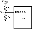 Figure 19. MODE_SEL Connection Diagram
Table 9. Configuration Select (MODE_SEL)
| NO. | IDEAL RATIO VR4/VDD33 |
IDEAL VR4
(V) |
SUGGESTED RESISTOR R3 kΩ (1% tolerance) | SUGGESTED RESISTOR R4 kΩ (1% tolerance) | LFMODE(1) | Repeater(2) | BACKWARD COMPATIBLE(3) |
I2S CHANNEL B (18–bit Mode)(4) |
|---|---|---|---|---|---|---|---|---|
| 1 | 0 | 0 | Open | 40.2 | L | L | L | L |
| 2 | 0.123 | 0.407 | 115 | 16.2 | L | L | L | H |
| 3 | 0.167 | 0.552 | 121 | 24.3 | L | H | L | L |
| 4 | 0.227 | 0.748 | 162 | 47.5 | L | H | L | H |
| 5 | 0.291 | 0.960 | 137 | 56.2 | H | L | L | L |
| 6 | 0.366 | 1.209 | 107 | 61.9 | H | L | L | H |
| 7 | 0.458 | 1.510 | 113 | 95.3 | H | H | L | L |
| 8 | 0.542 | 1.790 | 95.3 | 113 | H | H | L | H |
| 9 | 0.611 | 2.016 | 73.2 | 115 | L | L | H | L |
8.4.4 Repeater Application
The DS90UB925Q-Q1 and DS90UB926Q-Q1 can be configured to extend data transmission over multiple links to multiple display devices. Setting the devices into repeater mode provides a mechanism for transmitting to all receivers in the system.
In a repeater application, in this document, the DS90UB925Q-Q1 is referred to as the Transmitter or transmit port (TX), and the DS90UB926Q-Q1 is referred to as the Receiver (RX). Figure 20 shows the maximum configuration supported for Repeater implementations using the DS90UB925Q-Q1 (TX) and DS90UB926Q-Q1 (RX). Two levels of Repeaters are supported with a maximum of three Transmitters per Receiver.
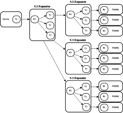 Figure 20. Maximum Repeater Application
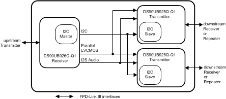 Figure 21. 1:2 Repeater Configuration
In a repeater application, the I2C interface at each TX and RX may be configured to transparently pass I2C communications upstream or downstream to any I2C device within the system. This includes a mechanism for assigning alternate IDs (Slave Aliases) to downstream devices in the case of duplicate addresses.
At each repeater node, the parallel LVCMOS interface fans out to up to three serializer devices, providing parallel RGB video data, HS/VS/DE control signals and, optionally, packetized audio data (transported during video blanking intervals). Alternatively, the I2S audio interface may be used to transport digital audio data between receiver and transmitters in place of packetized audio. All audio and video data is transmitted at the output of the Receiver and is received by the Transmitter..
Figure 21 provides more detailed block diagram of a 1:2 repeater configuration.
8.4.4.1 Repeater Connections
The Repeater requires the following connections between the Receiver and each Transmitter for Figure 22:
- Video Data – Connect PCLK, RGB and control signals (DE, VS, HS).
- I2C – Connect SCL and SDA signals. Both signals should be pulled up to VDD33 with 4.7-kΩ resistors.
- Audio – Connect I2S_CLK, I2S_WC, and I2S_DA signals.
- IDx pin – Each Transmitter and Receiver must have an unique I2C address.
- MODE_SEL pin – All Transmitter and Receiver must be set into the Repeater Mode.
- Interrupt pin– Connect DS90UB926Q-Q1 INTB_IN pin to DS90UB925Q-Q1 INTB pin. The signal must be pulled up to VDDIO.
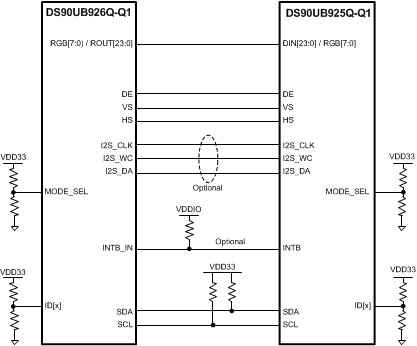 Figure 22. Repeater Connection Diagram
8.5 Programming
8.5.1 Serial Control Bus
The DS90UB926Q-Q1 is configured by the use of a serial control bus that is I2C protocol compatible. . Multiple deserializer devices may share the serial control bus since 16 device addresses are supported. Device address is set through the R1 and R2 values on IDx pin. See Figure 23.
The serial control bus consists of two signals and a configuration pin. The SCL is a Serial Bus Clock Input / Output. The SDA is the Serial Bus Data Input / Output signal. Both SCL and SDA signals require an external pullup resistor to VDD33. For most applications a 4.7-kΩ pullup resistor to VDD33 may be used. The resistor value may be adjusted for capacitive loading and data rate requirements. The signals are either pulled High, or driven Low.
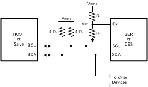 Figure 23. Serial Control Bus Connection
The configuration pin is the IDx pin. This pin sets one of 16 possible device addresses. A pullup resistor and a pulldown resistor of suggested values may be used to set the voltage ratio of the IDx input (VR2) and VDD33 to select one of the other 16 possible addresses. See Table 10.
Table 10. Serial Control Bus Addresses for IDx
8.6 Register Maps
Table 11. Serial Control Bus Registers
| ADD (dec) |
ADD (hex) |
Register Name | Bit(s) | Register Type |
Default (hex) |
Function | Descriptions |
|---|---|---|---|---|---|---|---|
| 0 | 0x00 | I2C Device ID | 7:1 | RW | Device ID | 7–bit address of Deserializer See Table 9 |
|
| 0 | RW | ID Setting | I2C ID Setting 1: Register I2C Device ID (Overrides IDx pin) 0: Device ID is from IDx pin |
||||
| 1 | 0x01 | Reset | 7 | RW | 0x04 | Remote Auto Power Down | Remote Auto Power Down 1: Power down when no forward channel link is detected 0: Do not power down when no forward channel link is detected |
| 6:3 | Reserved | ||||||
| 2 | RW | BC Enable | Back channel enable 1: Enable 0: Disable |
||||
| 1 | RW | Digital RESET1 | Reset the entire digital block including registers This bit is self-clearing. 1: Reset 0: Normal operation |
||||
| 0 | RW | Digital RESET0 | Reset the entire digital block except registers This bit is self-clearing 1: Reset 0: Normal operation |
||||
| 2 | 0x02 | Configuration [0] | 7 | RW | 0x00 | Output Enable | LVCMOS Output Enable. 1: Enable 0: Disable. Tri-state Outputs |
| 6 | RW | OEN and OSS_SEL Override | Overrides Output Enable Pin and Output State pin 1: Enable override 0: Disable - no override |
||||
| 5 | RW | OSC Clock Enable | OSC Clock Output Enable If loss of lock OSC clock is output onto PCLK 0: Disable 1: Enable |
||||
| 4 | RW | Output Sleep State Select (OSS_SEL) | OSS Select to Control Output State during Lock Low Period 1: Enable 0: Disable |
||||
| 3 | RW | Backward Compatible Mode Override | Mode_Sel Backward compatible Mode Override Enable. 1: Use register bit "reg_02[2]" to set BC Mode 0: Use MODE_SEL option. |
||||
| 2 | RW | Backward Compatible Mode Select | Backward Compatible Mode Select to DS90UR905Q and DS90UR907Q. If Reg_02[3] = 1 1: Backward Compatible is on 0: Backward Compatible is off |
||||
| 1 | RW | LFMODE Pin Override | LFMODE Pin Override Enable 1: Use register bit "reg_02[0]" to set LFMODE 0: Use LFMODE Pin |
||||
| 0 | RW | LFMODE | Low Frequency Mode Select 1: PCLK = 5 to <15 MHz 0: PCLK = 15 to 85 MHz |
||||
| 3 | 0x03 | Configuration [1] | 7 | 0xF0 | Reserved | ||
| 6 | RW | CRC Generator Enable | CRC Generator Enable (Back Channel) 1: Enable 0: Disable |
||||
| 5 | Reserved | ||||||
| 4 | RW | Filter Enable | HS, VS, DE two clock filter When enabled, pulses less than two full PCLK cycles on the DE, HS, and VS inputs will be rejected 1: Filtering enable 0: Filtering disable |
||||
| 3 | RW | I2C Pass-through | I2C Pass-Through Mode 1: Pass-Through Enabled 0: Pass-Through Disabled |
||||
| 2 | RW | Auto ACK | ACK Select 1: Auto ACK enable 0: Self ACK |
||||
| 1 | Reserved | ||||||
| 0 | RW | RRFB | Pixel Clock Edge Select 1: Parallel Interface Data is strobed on the Rising Clock Edge. 0: Parallel Interface Data is strobed on the Falling Clock Edge. |
||||
| 4 | 0x04 | BCC Watchdog Control | 7:1 | RW | 0xFE | BCC Watchdog Timer | The watchdog timer allows termination of a control channel transaction, if it fails to complete within a programmed amount of time. This field sets the Bidirectional Control Channel Watchdog Timeout value in units of 2 milliseconds. This field should not be set to 0 |
| 0 | RW | BCC Watchdog Timer Disable | Disable Bidirectional Control Channel Watchdog Timer 1: Disables BCC Watchdog Timer operation 0: Enables BCC Watchdog Timer operation" |
||||
| 5 | 0x05 | I2C Control [1] | 7 | RW | 0x2E | I2C Pass Through All | I2C Pass-Through All Transactions 1: Enabled 0: Disabled |
| 6:4 | RW | I2C SDA Hold Time | Internal I2C SDA Hold Time It configures the amount of internal hold time provided for the SDA input relative to the SCL input. Units are 50 ns. |
||||
| 3:0 | RW | I2C Filter Depth | I2C Glitch Filter Depth It configures the maximum width of glitch pulses on the SCL and SDA inputs that will be rejected. Units are 5 ns. |
||||
| 6 | 0x06 | I2C Control [2] | 7 | R | 0x00 | Forward Channel Sequence Error | Control Channel Sequence Error Detected It indicates a sequence error has been detected in forward control channel. It this bit is set, an error may have occurred in the control channel operation. |
| 6 | RW | Clear Sequence Error | It clears the Sequence Error Detect bit This bit is not self-clearing. |
||||
| 5 | Reserved | ||||||
| 4:3 | RW | SDA Output Delay | SDA Output Delay This field configures output delay on the SDA output. Setting this value will increase output delay in units of 50 ns. Nominal output delay values for SCL to SDA are: 00 : 250 ns 01: 300 ns 10: 350 ns 11: 400 ns |
||||
| 2 | RW | Local Write | Disable Remote Writes to Local Registers through Serializer (Does not affect remote access to I2C slaves at Deserializer) 1: Stop remote write to local device registers 0: remote write to local device registers |
||||
| 1 | RW | I2C Bus Timer Speed | Speed up I2C Bus Watchdog Timer 1: Timer expires after approximately 50 ms 0: Timer expires after approximately 1 s |
||||
| 0 | RW | I2C Bus Timer Disable | Disable I2C Bus Timer When the I2C Timer may be used to detect when the I2C bus is free or hung up following an invalid termination of a transaction. If SDA is high and no signalling occurs for approximately 1 s, the I2C bus is assumed to be free. If SDA is low and no signaling occurs, the device will try to clear the bus by driving 9 clocks on SCL | ||||
| 7 | 0x07 | Remote Device ID | 7:1 | RW | 0x18 | Remote ID | Remote ID Configures the I2C Slave ID of the remote Serializer. A value of 0 in this field disables I2C access to remote Serializer. This field is automatically configured through the Serializer Forward Channel. Software may overwrite this value, but should also set the FREEZE DEVICE ID bit to prevent overwriting by the Forward Channel. |
| 0 | RW | Freeze Device ID | Freeze Serializer Device ID 1: Prevent auto-loading of the Serializer Device ID from the Forward Channel. The ID will be frozen at the value written. 0: Update |
||||
| 8 | 0x08 | SlaveID[0] | 7:1 | RW | 0x00 | Target Slave Device ID0 | 7-bit Remote Slave Device ID 0 Configures the physical I2C address of the remote I2C Slave device attached to the remote Serializer. If an I2C transaction is addressed to the Slave Alias ID0, the transaction will be remapped to this address before passing the transaction across the Bidirectional Control Channel to the Serializer. |
| 0 | Reserved | ||||||
| 9 | 0x09 | SlaveID[1] | 7:1 | RW | 0x00 | Target Slave Device ID1 | 7-bit Remote Slave Device ID 1 Configures the physical I2C address of the remote I2C Slave device attached to the remote Serializer. If an I2C transaction is addressed to the Slave Alias ID1, the transaction will be remapped to this address before passing the transaction across the Bidirectional Control Channel to the Serializer. |
| 0 | Reserved | ||||||
| 10 | 0x0A | SlaveID[2] | 7:1 | RW | 0x00 | Target Slave Device ID2 | 7-bit Remote Slave Device ID 2 Configures the physical I2C address of the remote I2C Slave device attached to the remote Serializer. If an I2C transaction is addressed to the Slave Alias ID2, the transaction will be remapped to this address before passing the transaction across the Bidirectional Control Channel to the Serializer. |
| 0 | Reserved | ||||||
| 11 | 0x0B | SlaveID[3] | 7:1 | RW | 0x00 | Target Slave Device ID3 | 7-bit Remote Slave Device ID 3 Configures the physical I2C address of the remote I2C Slave device attached to the remote Serializer. If an I2C transaction is addressed to the Slave Alias ID3, the transaction will be remapped to this address before passing the transaction across the Bidirectional Control Channel to the Serializer. |
| 0 | Reserved | ||||||
| 12 | 0x0C | SlaveID[4] | 7:1 | RW | 0x00 | Target Slave Device ID4 | 7-bit Remote Slave Device ID 4 Configures the physical I2C address of the remote I2C Slave device attached to the remote Serializer. If an I2C transaction is addressed to the Slave Alias ID4, the transaction will be remapped to this address before passing the transaction across the Bidirectional Control Channel to the Serializer. |
| 0 | Reserved | ||||||
| 13 | 0x0D | SlaveID[5] | 7:1 | RW | 0x00 | Target Slave Device ID5 | 7-bit Remote Slave Device ID 5 Configures the physical I2C address of the remote I2C Slave device attached to the remote Serializer. If an I2C transaction is addressed to the Slave Alias ID5, the transaction will be remapped to this address before passing the transaction across the Bidirectional Control Channel to the Serializer. |
| 0 | Reserved | ||||||
| 14 | 0x0E | SlaveID[6] | 7:1 | RW | 0x00 | Target Slave Device ID6 | 7-bit Remote Slave Device ID 6 Configures the physical I2C address of the remote I2C Slave device attached to the remote Serializer. If an I2C transaction is addressed to the Slave Alias ID6, the transaction will be remapped to this address before passing the transaction across the Bidirectional Control Channel to the Serializer. |
| 0 | Reserved | ||||||
| 15 | 0x0F | SlaveID[7] | 7:1 | RW | 0x00 | Target Slave Device ID7 | 7-bit Remote Slave Device ID 7 Configures the physical I2C address of the remote I2C Slave device attached to the remote Serializer. If an I2C transaction is addressed to the Slave Alias ID7, the transaction will be remapped to this address before passing the transaction across the Bidirectional Control Channel to the Serializer. |
| 0 | Reserved | ||||||
| 16 | 0x10 | SlaveAlias[0] | 7:1 | RW | 0x00 | ID[0] Match | 7-bit Remote Slave Device Alias ID 0 Configures the decoder for detecting transactions designated for an I2C Slave device attached to the remote Serializer. The transaction will be remapped to the address specified in the Slave ID0 register. A value of 0 in this field disables access to the remote I2C Slave. |
| 0 | Reserved | ||||||
| 17 | 0x11 | SlaveAlias[1] | 7:1 | RW | 0x00 | ID[1] Match | 7-bit Remote Slave Device Alias ID 1 Configures the decoder for detecting transactions designated for an I2C Slave device attached to the remote Serializer. The transaction will be remapped to the address specified in the Slave ID1 register. A value of 0 in this field disables access to the remote I2C Slave. |
| 0 | Reserved | ||||||
| 18 | 0x12 | SlaveAlias[2] | 7:1 | RW | 0x00 | ID[2] Match | 7-bit Remote Slave Device Alias ID 2 Configures the decoder for detecting transactions designated for an I2C Slave device attached to the remote Serializer. The transaction will be remapped to the address specified in the Slave ID2 register. A value of 0 in this field disables access to the remote I2C Slave. |
| 0 | Reserved | ||||||
| 19 | 0x13 | SlaveAlias[3] | 7:1 | RW | 0x10 | ID[3] Match | 7-bit Remote Slave Device Alias ID 3 Configures the decoder for detecting transactions designated for an I2C Slave device attached to the remote Serializer. The transaction will be remapped to the address specified in the Slave ID3 register. A value of 0 in this field disables access to the remote I2C Slave. |
| 0 | Reserved | ||||||
| 20 | 0x14 | SlaveAlias[4] | 7:1 | RW | 0x00 | ID[4] Match | 7-bit Remote Slave Device Alias ID 4 Configures the decoder for detecting transactions designated for an I2C Slave device attached to the remote Serializer. The transaction will be remapped to the address specified in the Slave ID4 register. A value of 0 in this field disables access to the remote I2C Slave. |
| 0 | Reserved | ||||||
| 21 | 0x15 | SlaveAlias[5] | 7:1 | RW | 0x00 | ID[5] Match | 7-bit Remote Slave Device Alias ID 5 Configures the decoder for detecting transactions designated for an I2C Slave device attached to the remote Serializer. The transaction will be remapped to the address specified in the Slave ID5 register. A value of 0 in this field disables access to the remote I2C Slave. |
| 0 | Reserved | ||||||
| 22 | 0x16 | SlaveAlias[6] | 7:1 | RW | 0x00 | ID[6] Match | 7-bit Remote Slave Device Alias ID 6 Configures the decoder for detecting transactions designated for an I2C Slave device attached to the remote Serializer. The transaction will be remapped to the address specified in the Slave ID6 register. A value of 0 in this field disables access to the remote I2C Slave. |
| 0 | RW | Reserved | |||||
| 23 | 0x17 | SlaveAlias[7] | 7:1 | RW | 0x00 | ID[7] Match | 7-bit Remote Slave Device Alias ID 7 Configures the decoder for detecting transactions designated for an I2C Slave device attached to the remote Serializer. The transaction will be remapped to the address specified in the Slave ID7 register. A value of 0 in this field disables access to the remote I2C Slave. |
| 0 | Reserved | ||||||
| 28 | 0x1C | General Status | 7:4 | RW | 0x00 | Reserved | |
| 3 | R | I2S Locked | I2S Lock Status 0: I2S PLL controller not locked 1: I2S PLL controller locked to input I2S clock |
||||
| 2 | Reserved | ||||||
| 1 | Reserved | ||||||
| 0 | R | Lock | Deserializer CDR, PLL's clock to recovered clock frequency 1: Deserializer locked to recovered clock 0: Deserializer not locked |
||||
| 29 | 0x1D | GPIO0 Config | 7:4 | R | 0xA0 | Rev-ID | Revision ID: 1010: Production Device |
| 3 | RW | GPIO0 Output Value | Local GPIO Output Value This value is output on the GPIO pin when the GPIO function is enabled, the local GPIO direction is Output, and remote GPIO control is disabled. |
||||
| 2 | RW | GPIO0 Remote Enable | Remote GPIO0 Control 1: Enable GPIO control from remote Serializer. The GPIO pin will be an output, and the value is received from the remote Deserializer. 0: Disable GPIO control from remote Serializer |
||||
| 1 | RW | GPIO0 Direction | Local GPIO Direction 1: Input 0: Output |
||||
| 0 | RW | GPIO0 Enable | GPIO Function Enable 1: Enable GPIO operation 0: Enable normal operation |
||||
| 30 | 0x1E | GPIO2 and GPIO1 Config | 7 | RW | 0x00 | GPIO2 Output Value | Local GPIO Output Value This value is output on the GPIO when the GPIO function is enabled, the local GPIO direction is Output, and remote GPIO control is disabled. |
| 6 | RW | GPIO2 Remote Enable | Remote GPIO2 Control 1: Enable GPIO control from remote Serializer. The GPIO pin will be an output, and the value is received from the remote Deserializer. 0: Disable GPIO control from remote Serializer. |
||||
| 5 | RW | GPIO2 Direction | Local GPIO Direction 1: Input 0: Output |
||||
| 4 | RW | GPIO2 Enable | GPIO Function Enable 1: Enable GPIO operation 0: Enable normal operation |
||||
| 3 | RW | GPIO1 Output Value | Local GPIO Output Value This value is output on the GPIO when the GPIO function is enabled, the local GPIO direction is Output, and remote GPIO control is disabled. |
||||
| 2 | RW | GPIO1 Remote Enable | Remote GPIO1 Control 1: Enable GPIO control from remote Serializer. The GPIO pin will be an output, and the value is received from the remote Deserializer. 0: Disable GPIO control from remote Serializer. |
||||
| 1 | RW | GPIO1 Direction | Local GPIO Direction 1: Input 0: Output |
||||
| 0 | RW | GPIO1 Enable | GPIO Function Enable 1: Enable GPIO operation 0: Enable normal operation |
||||
| 31 | 0x1F | GPO_REG4 and GPO3 Config | 7 | RW | 0x00 | GPO_REG4 Output Value | Local GPO_REG4 Output Value This value is output on the GPO when the GPO function is enabled, the local GPO direction is Output, and remote GPO control is disabled. |
| 6:5 | Reserved | ||||||
| 4 | RW | GPO_REG4 Enable | GPO_REG4 Function Enable 1: Enable GPO operation 0: Enable normal operation |
||||
| 3 | RW | GPIO3 Output Value | Local GPIO Output Value This value is output on the GPIO when the GPIO function is enabled, the local GPIO direction is Output, and remote GPIO control is disabled. | ||||
| 2 | RW | GPIO3 Remote Enable | Remote GPIO3 Control 1: Enable GPIO control from remote Serializer. The GPIO pin will be an output, and the value is received from the remote Deserializer. 0: Disable GPIO control from remote Serializer. |
||||
| 1 | RW | GPIO3 Direction | Local GPIO Direction 1: Input 0: Output |
||||
| 0 | RW | GPIO3 Enable | GPIO Function Enable 1: Enable GPIO operation 0: Enable normal operation |
||||
| 32 | 0x20 | GPO_REG6 and GPO_REG5 Config | 7 | RW | 0x00 | GPO_REG6 Output Value | Local GPO_REG6 Output Value This value is output on the GPO when the GPO function is enabled, the local GPO direction is Output, and remote GPO control is disabled. |
| 6:5 | Reserved | ||||||
| 4 | RW | GPO_REG6 Enable | GPO_REG6 Function Enable 1: Enable GPO operation 0: Enable normal operation |
||||
| 3 | RW | GPO_REG5 Output Value | Local GPO_REG5 Output Value This value is output on the GPO when the GPO function is enabled, the local GPO direction is Output, and remote GPO control is disabled. |
||||
| 2:1 | Reserved | ||||||
| 0 | RW | GPO_REG5 Enable | GPO_REG5 Function Enable 1: Enable GPO operation 0: Enable normal operation |
||||
| 33 | 0x21 | GPO8 and GPO7 Config | 7 | RW | 0x00 | GPO_REG8 Output Value | Local GPO_REG8 Output Value This value is output on the GPO when the GPO function is enabled, the local GPO direction is Output, and remote GPO control is disabled. |
| 6:5 | Reserved | ||||||
| 4 | RW | GPO_REG8 Enable | GPO_REG8 Function Enable 1: Enable GPO operation 0: Enable normal operation |
||||
| 3 | RW | GPO_REG7 Output Value | Local GPO_REG7 Output Value This value is output on the GPO when the GPO function is enabled, the local GPO direction is Output, and remote GPO control is disabled. |
||||
| 2:1 | Reserved | ||||||
| 0 | RW | GPO_REG7 Enable | GPO_REG7 Function Enable 1: Enable GPO operation 0: Enable normal operation |
||||
| 34 | 0x22 | Data Path Control | 7 | RW | 0x00 | Override FC Config | 1: Disable loading of this register from the forward channel, keeping locally written values intact 0: Allow forward channel loading of this register |
| 6 | RW | Pass RGB | Setting this bit causes RGB data to be sent independent of DE. This allows operation in systems which may not use DE to frame video data or send other data when DE is deasserted. Note that setting this bit blocks packetized audio. This bit does not need to be set in DS90UB925 or in Backward Compatibility mode. 1: Pass RGB independent of DE 0: Normal operation Note: this bit is automatically loaded from the remote serializer unless bit 7 of this register is set. |
||||
| 5 | RW | DE Polarity | This bit indicates the polarity of the DE (Data Enable) signal. 1: DE is inverted (active low, idle high) 0: DE is positive (active high, idle low) Note: this bit is automatically loaded from the remote serializer unless bit 7 of this register is set. |
||||
| 4 | RW | I2S_Gen | This bit controls whether the Receiver outputs packetized Auxiliary/Audio data on the RGB video output pins. 1: Don't output packetized audio data on RGB video output pins 0: Output packetized audio on RGB video output pins. Note: this bit is automatically loaded from the remote serializer unless bit 7 of this register is set. |
||||
| 3 | RW | I2S Channel B Enable Override | 1: Set I2S Channel B Enable from reg_22[0] 0: Set I2S Channel B Enable from MODE_SEL pin Note: this bit is automatically loaded from the remote serializer unless bit 7 of this register is set. |
||||
| 2 | RW | 18-bit Video Select | 1: Select 18-bit video mode 0: Select 24-bit video mode Note: this bit is automatically loaded from the remote serializer unless bit 7 of this register is set. |
||||
| 1 | RW | I2S Transport Select | 1: Enable I2S Data Forward Channel Frame Transport 0: Enable I2S Data Island Transport Note: this bit is automatically loaded from the remote serializer unless bit 7 of this register is set. |
||||
| 0 | RW | I2S Channel B Enable | I2S Channel B Enable 1: Enable I2S Channel B on B1 output 0: I2S Channel B disabled Note: this bit is automatically loaded from the remote serializer unless bit 7 of this register is set. |
||||
| 35 | 0x23 | General Purpose Control | 7 | RW | 0x10 | Rx RGB Checksum | RX RGB Checksum Enable Setting this bit enables the Receiver to validate a one-byte checksum following each video line. Checksum failures are reported in the STS register |
| 6:5 | Reserved | ||||||
| 4 | R | Mode_Sel | Mode Select is Done | ||||
| 3 | R | LFMODE | Low Frequency Mode Status | ||||
| 2 | R | Repeater | Repeater Mode Status | ||||
| 1 | R | Backward | Backward Compatible Mode Status | ||||
| 0 | R | I2S Channel B | I2S Channel B Status | ||||
| 36 | 0x24 | BIST Control | 7:4 | 0x08 | Reserved | ||
| 3 | RW | BIST Pin Config | BIST Configured through Pin 1: BIST configured through pin 0: BIST configured through register bit |
||||
| 2:1 | RW | BIST Clock Source | BIST Clock Source 00: External Pixel Clock 01: 33 MHz Oscillator 10: Reserved 11: 25 MHz Oscillator |
||||
| 0 | RW | BIST Enable | BIST Control 1: Enabled 0: Disabled |
||||
| 37 | 0x25 | BIST Error | 7:0 | R | 0x00 | BIST Error Count | BIST Error Count |
| 38 | 0x26 | SCL High Time | 7:0 | RW | 0x83 | SCL High Time | I2C Master SCL High Time This field configures the high pulse width of the SCL output when the Deserializer is the Master on the local I2C bus. Units are 50 ns for the nominal oscillator clock frequency. The default value is set to provide a minimum 5us SCL high time with the internal oscillator clock running at 26 MHz rather than the nominal 20 MHz. |
| 39 | 0x27 | SCL Low Time | 7:0 | RW | 0x84 | SCL Low Time | I2C SCL Low Time This field configures the low pulse width of the SCL output when the De-Serializer is the Master on the local I2C bus. This value is also used as the SDA setup time by the I2C Slave for providing data prior to releasing SCL during accesses over the Bidirectional Control Channel. Units are 50 ns for the nominal oscillator clock frequency. The default value is set to provide a minimum 5us SCL low time with the internal oscillator clock running at 26 MHz rather than the nominal 20 MHz. |
| 41 | 0x29 | FRC Control | 7 | RW | 0x00 | Timing Mode Select | Select display timing mode 0: DE only Mode 1: Sync Mode (VS,HS) |
| 6 | RW | VS Polarity | 0: Active High 1: Active Low |
||||
| 5 | RW | HS Polarity | 0: Active High 1: Active Low |
||||
| 4 | RW | DE Polarity | 0: Active High 1: Active Low |
||||
| 3 | RW | FRC2 Enable | 0: FRC2 Disable 1: FRC2 Enable |
||||
| 2 | RW | FRC1 Enable | 0: FRC1 Disable 1: FRC1 Enable |
||||
| 1 | RW | Hi-FRC 2 Disable | 0: Hi-FRC2 Enable 1: Hi-FRC2 Disable |
||||
| 0 | RW | Hi-FRC 1 Disable | 0: Hi-FRC1 Enable 1: Hi-FRC1 Disable |
||||
| 42 | 0x2A | White Balance Control | 7:6 | RW | 0x00 | Page Setting | 00: Configuration Registers 01: Red LUT 10: Green LUT 11: Blue LUT |
| 5 | RW | White Balance Enable | 0: White Balance Disable 1: White Balance Enable |
||||
| 4 | RW | LUT Reload Enable | 0: Reload Disable 1: Reload Enable |
||||
| 3:0 | Reserved | ||||||
| 43 | 0x2B | I2S Control | 7 | RW | 0x00 | I2S PLL | I2S PLL Control 0: I2S PLL is on for I2S data jitter cleaning 1: I2S PLL is off. No jitter cleaning |
| 6:1 | Reserved | ||||||
| 0 | RW | I2S Clock Edge | I2S Clock Edge Select 0: I2S Data is strobed on the Rising Clock Edge 1: I2S Data is strobed on the Falling Clock Edge |
||||
| 44 | 0x2C | SSCG Control | 7:4 | 0x00 | Reserved | ||
| 3 | RW | SSCG Enable | Enable Spread Spectrum Clock Generator 0: Disable 1: Enable |
||||
| 2:0 | RW | SSCG Selection | SSCG Frequency Deviation: When LFMODE = H fdev fmod 000: ±0.7 CLK/628 001: ±1.3 010: ±1.8 011: ±2.5 100: ±0.7 CLK/388 101: ±1.2 110: ±2 111: ±2.5 When LFMODE = L fdev fmod 000: ±0.9 CLK/2168 001: ±1.2 010: ±1.9 011: ±2.5 100: ±0.7 CLK/1300 101: ±1.3 110: ±2 111: ±2.5 |
||||
| 58 | 0x3A | I2S MCLK Output | 7 | RW | 0x00 | MCLK Override | 1: Override divider select for MCLK 0: No override for MCLK divider |
| 6:4 | RW | MCLK Frequency Select | See Table 5 | ||||
| 3:0 | Reserved | ||||||
| 65 | 0x41 | Link Error Count | 7:5 | 0x03 | Reserved | ||
| 4 | RW | Link Error Count Enable | Enable serial link data integrity error count 1: Enable error count 0: Disable |
||||
| 3:0 | RW | Link Error Count | Link error count threshold. Counter is pixel clock based. clk0, clk1 and DCA are monitored for link errors, if error count is enabled, deserializer loose lock once error count reaches threshold. If disabled deserilizer loose lock with one error. |
||||
| 68 | 0x44 | Equalization | 7:5 | RW | 0x60 | EQ Stage 1 Select | EQ select value. Used if adaptive EQ is bypassed. 000 Min EQ 1st Stage 001 010 011 100 101 110 111 Max EQ 1st Stage |
| 4 | Reserved | ||||||
| 3:1 | RW | EQ Stage 2 Select | EQ select value. Used if adaptive EQ is bypassed. 000 Min EQ 2nd Stage 001 010 011 100 101 110 111 Max EQ 2nd Stage |
||||
| 0 | RW | Adaptive EQ | 1: Disable adaptive EQ (to write EQ select values) 0: Enable adaptive EQ |
||||
| 86 | 0x56 | CML Output | 7:4 | 0x08 | Reserved | ||
| 3 | RW | CMLOUT+/- Enable | 1: Disabled (Default) 0: Enabled |
||||
| 2:0 | Reserved | ||||||
| 100 | 0x64 | Pattern Generator Control | 7:4 | RW | 0x10 | Pattern Generator Select | Fixed Pattern Select This field selects the pattern to output when in Fixed Pattern Mode. Scaled patterns are evenly distributed across the horizontal or vertical active regions. This field is ignored when Auto-Scrolling Mode is enabled. The following table shows the color selections in non-inverted followed by inverted color mode 0000: Reserved 0001: White/Black 0010: Black/White 0011: Red/Cyan 0100: Green/Magenta 0101: Blue/Yellow 0110: Horizontally Scaled Black to White/White to Black 0111: Horizontally Scaled Black to Red/Cyan to White 1000: Horizontally Scaled Black to Green/Magenta to White 1001: Horizontally Scaled Black to Blue/Yellow to White 1010: Vertically Scaled Black to White/White to Black 1011: Vertically Scaled Black to Red/Cyan to White 1100: Vertically Scaled Black to Green/Magenta to White 1101: Vertically Scaled Black to Blue/Yellow to White 1110: Custom color (or its inversion) configured in PGRS, PGGS, PGBS registers 1111: Reserved |
| 3:1 | Reserved | ||||||
| 0 | RW | Pattern Generator Enable | Pattern Generator Enable 1: Enable Pattern Generator 0: Disable Pattern Generator |
||||
| 101 | 0x65 | Pattern Generator Configuration | 7:5 | 0x00 | Reserved | ||
| 4 | RW | Pattern Generator 18 Bits | 18-bit Mode Select 1: Enable 18-bit color pattern generation. Scaled patterns will have 64 levels of brightness and the R, G, and B outputs use the six most significant color bits. 0: Enable 24-bit pattern generation. Scaled patterns use 256 levels of brightness. |
||||
| 3 | RW | Pattern Generator External Clock | Select External Clock Source 1: Selects the external pixel clock when using internal timing. 0: Selects the internal divided clock when using internal timing This bit has no effect in external timing mode (PATGEN_TSEL = 0). |
||||
| 2 | RW | Pattern Generator Timing Select | Timing Select Control 1: The Pattern Generator creates its own video timing as configured in the Pattern Generator Total Frame Size, Active Frame Size. Horizontal Sync Width, Vertical Sync Width, Horizontal Back Porch, Vertical Back Porch, and Sync Configuration registers. 0: the Pattern Generator uses external video timing from the pixel clock, Data Enable, Horizontal Sync, and Vertical Sync signals. |
||||
| 1 | RW | Pattern Generator Color Invert | Enable Inverted Color Patterns 1: Invert the color output. 0: Do not invert the color output. |
||||
| 0 | RW | Pattern Generator Auto-Scroll Enable | Auto-Scroll Enable: 1: The Pattern Generator will automatically move to the next enabled pattern after the number of frames specified in the Pattern Generator Frame Time (PGFT) register. 0: The Pattern Generator retains the current pattern. |
||||
| 102 | 0x66 | Pattern Generator Indirect Address | 7:0 | RW | 0x00 | Indirect Address | This 8-bit field sets the indirect address for accesses to indirectly-mapped registers. It should be written prior to reading or writing the Pattern Generator Indirect Data register. See AN-2198 Exploring Int Test Patt Gen Feat of 720p FPD-Link III Devices (SNLA132) |
| 103 | 0x67 | Pattern Generator Indirect Data | 7:0 | RW | 0x00 | Indirect Data | When writing to indirect registers, this register contains the data to be written. When reading from indirect registers, this register contains the read back value. See AN-2198 Exploring Int Test Patt Gen Feat of 720p FPD-Link III Devices (SNLA132) |
| 240 | 0xF0 | RX ID | 7:0 | R | 0x5F | ID0 | First byte ID code: _ |
| 241 | 0xF1 | 7:0 | R | 0x55 | ID1 | Second byte of ID code: U | |
| 242 | 0xF2 | 7:0 | R | 0x48 | ID2 | Third byte of ID code, Value will be either B. | |
| 243 | 0xF3 | 7:0 | R | 0x39 | ID3 | Fourth byte of ID code: 9 | |
| 244 | 0xF4 | 7:0 | R | 0x32 | ID4 | Fifth byte of ID code: 2 | |
| 245 | 0xF5 | 7:0 | R | 0x36 | ID5 | Sixth byte of ID code: 6 |