ZHCSDB9C August 2013 – February 2017 ADS1120
PRODUCTION DATA.
- 1 特性
- 2 应用
- 3 说明
- 4 修订历史记录
- 5 Pin Configuration and Functions
- 6 Specifications
- 7 Parameter Measurement Information
-
8 Detailed Description
- 8.1 Overview
- 8.2 Functional Block Diagram
- 8.3 Feature Description
- 8.4 Device Functional Modes
- 8.5 Programming
- 8.6 Register Map
- 9 Application and Implementation
- 10Power Supply Recommendations
- 11Layout
- 12器件和文档支持
- 13机械、封装和可订购信息
8 Detailed Description
8.1 Overview
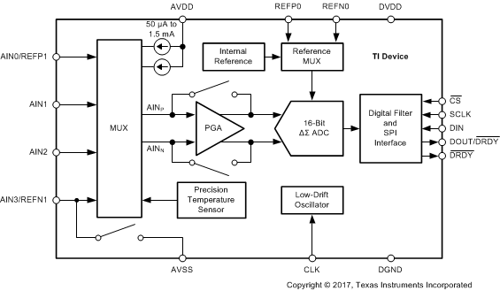
The ADS1120 is a small, low-power, 16-bit, ΔΣ ADC that offers many integrated features to reduce system cost and component count in applications measuring small sensor signals.
In addition to the ΔΣ ADC core and single-cycle settling digital filter, the device offers a low-noise, high input impedance, programmable gain amplifier (PGA), an internal voltage reference, and a clock oscillator. The device also integrates a highly linear and accurate temperature sensor as well as two matched programmable current sources (IDACs) for sensor excitation. All of these features are intended to reduce the required external circuitry in typical sensor applications and improve overall system performance. An additional low-side power switch eases the design of low-power bridge sensor applications. The device is fully configured through four registers and controlled by six commands through a mode 1 SPI-compatible interface. The Functional Block Diagram section shows the device functional block diagram.
The ADS1120 ADC measures a differential signal, VIN, which is the difference in voltage between nodes AINP and AINN. The converter core consists of a differential, switched-capacitor, ΔΣ modulator followed by a digital filter. The digital filter receives a high-speed bitstream from the modulator and outputs a code proportional to the input voltage. This architecture results in a very strong attenuation of any common-mode signal.
The device has two available conversion modes: single-shot and continuous conversion mode. In single-shot mode, the ADC performs one conversion of the input signal upon request and stores the value in an internal data buffer. The device then enters a low-power state to save power. Single-shot mode is intended to provide significant power savings in systems that require only periodic conversions, or when there are long idle periods between conversions. In continuous conversion mode, the ADC automatically begins a conversion of the input signal as soon as the previous conversion is completed. New data are available at the programmed data rate. Data can be read at any time without concern of data corruption and always reflect the most recently completed conversion.
8.3 Feature Description
8.3.1 Multiplexer
The device contains a very flexible input multiplexer, as shown in Figure 38. Either four single-ended signals, two differential signals, or a combination of two single-ended signals and one differential signal can be measured. The multiplexer is configured by four bits (MUX[3:0]) in the configuration register. When single-ended signals are measured, the negative ADC input (AINN) is internally connected to AVSS by a switch within the multiplexer. For system-monitoring purposes, the analog supply (AVDD – AVSS) / 4 or the currently-selected external reference voltage (V(REFPx) – V(REFNx)) / 4 can be selected as inputs to the ADC. The multiplexer also offers the possibility to route any of the two programmable current sources to any analog input (AINx) or to any dedicated reference pin (REFP0, REFN0).
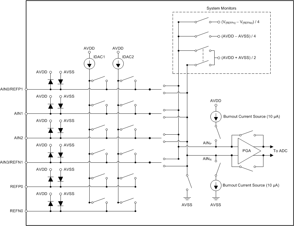 Figure 38. Analog Input Multiplexer
Electrostatic discharge (ESD) diodes to AVDD and AVSS protect the inputs. To prevent the ESD diodes from turning on, the absolute voltage on any input must stay within the range provided by Equation 4:
If the voltages on the input pins have any potential to violate these conditions, external Schottky clamp diodes or series resistors may be required to limit the input current to safe values (see the Absolute Maximum Ratings table). Overdriving an unused input on the device may affect conversions taking place on other input pins. If any overdrive on unused inputs is possible, TI recommends clamping the signal with external Schottky diodes.
8.3.2 Low-Noise PGA
The device features a low-noise, low-drift, high input impedance, programmable gain amplifier (PGA). The PGA can be set to gains of 1, 2, 4, 8, 16, 32, 64, or 128. Three bits (GAIN[2:0]) in the configuration register are used to configure the gain. A simplified diagram of the PGA is shown in Figure 39. The PGA consists of two chopper-stabilized amplifiers (A1 and A2) and a resistor feedback network that sets the PGA gain. The PGA input is equipped with an electromagnetic interference (EMI) filter.
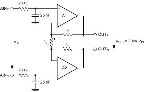 Figure 39. Simplified PGA Diagram
VIN denotes the differential input voltage VIN = (V(AINP) – V(AINN)). The gain of the PGA can be calculated with Equation 5:
Gain is changed inside the device using a variable resistor, RG. The differential full-scale input voltage range (FSR) of the PGA is defined by the gain setting and the reference voltage used, as shown in Equation 6:
Table 9 shows the corresponding full-scale ranges when using the internal 2.048-V reference.
Table 9. PGA Full-Scale Range
| GAIN SETTING | FSR |
|---|---|
| 1 | ±2.048 V |
| 2 | ±1.024 V |
| 4 | ±0.512 V |
| 8 | ±0.256 V |
| 16 | ±0.128 V |
| 32 | ±0.064 V |
| 64 | ±0.032 V |
| 128 | ±0.016 V |
8.3.2.1 PGA Common-Mode Voltage Requirements
To stay within the linear operating range of the PGA, the input signals must meet certain requirements that are discussed in this section.
The outputs of both amplifiers (A1 and A2) in Figure 39 can not swing closer to the supplies (AVSS and AVDD) than 200 mV. If the outputs OUTP and OUTN are driven to within 200 mV of the supply rails, the amplifiers saturate and consequently become nonlinear. To prevent this nonlinear operating condition the output voltages must meet Equation 7:
Translating the requirements of Equation 7 into requirements referred to the PGA inputs (AINP and AINN) is beneficial because there is no direct access to the outputs of the PGA. The PGA employs a symmetrical design, therefore the common-mode voltage at the output of the PGA can be assumed to be the same as the common-mode voltage of the input signal, as shown in Figure 40.
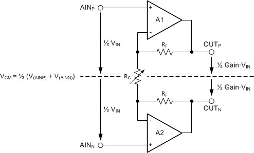 Figure 40. PGA Common-Mode Voltage
The common-mode voltage is calculated using Equation 8:
The voltages at the PGA inputs (AINP and AINN) can be expressed as Equation 9 and Equation 10:
The output voltages (V(OUTP) and V(OUTN)) can then be calculated as Equation 11 and Equation 12:
The requirements for the output voltages of amplifiers A1 and A2 (Equation 7) can now be translated into requirements for the input common-mode voltage range using Equation 11 and Equation 12, which are given in Equation 13 and Equation 14:
In order to calculate the minimum and maximum common-mode voltage limits, the maximum differential input voltage (VIN (MAX)) that occurs in the application must be used. VIN (MAX) can be less than the maximum possible FS value.
In addition to Equation 13, the minimum VCM must also meet Equation 15 because of the specific design implementation of the PGA.
Figure 41 and Figure 42 show a graphical representation of the common-mode voltage limits for AVDD = 3.3 V and AVSS = 0 V, with gain = 1 and gain = 16, respectively.
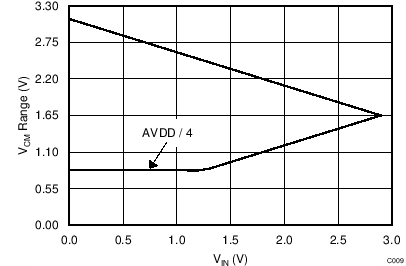
| AVDD = 3.3 V |
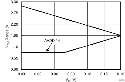
| AVDD = 3.3 V |
The following discussion explains how to apply Equation 13 through Equation 15 to a hypothetical application. The setup for this example is AVDD = 3.3 V, AVSS = 0 V, and gain = 16, using an external reference,
Vref = 2.5 V. The maximum possible differential input voltage VIN = (V(AINP) – V(AINN)) that can be applied is then limited to the full-scale range of FSR = ±2.5 V / 16 = ±0.156 V. Consequently, Equation 13 through Equation 15 yield an allowed VCM range of 1.45 V ≤ VCM ≤ 1.85 V.
If the sensor signal connected to the inputs in this hypothetical application does not make use of the entire full-scale range but is limited to VIN (MAX) = ±0.1 V, for example, then this reduced input signal amplitude relaxes the VCM restriction to 1.0 V ≤ VCM ≤ 2.3 V.
In the case of a fully-differential sensor signal, each input (AINP, AINN) can swing up to ±50 mV around the common-mode voltage (V(AINP) + V(AINN)) / 2, which must remain between the limits of 1.0 V and 2.3 V. The output of a symmetrical wheatstone bridge is an example of a fully-differential signal. Figure 43 shows a situation where the common-mode voltage of the input signal is at the lowest limit. V(OUTN) is exactly at 0.2 V in this case. Any further decrease in common-mode voltage (VCM) or increase in differential input voltage (VIN) drives V(OUTN) below 0.2 V and saturates amplifier A2.
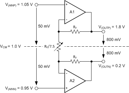 Figure 43. Example where VCM is at Lowest Limit
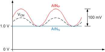
In contrast, the signal of an RTD is of a pseudo-differential nature (if implemented as shown in the RTD Measurement section), where the negative input is held at a constant voltage other than 0 V and only the voltage on the positive input changes. When a pseudo-differential signal must be measured, the negative input in this example must be biased at a voltage between 0.95 V and 2.25 V. The positive input can then swing up to
VIN (MAX) = 100 mV above the negative input. Note that in this case the common-mode voltage changes at the same time the voltage on the positive input changes. That is, while the input signal swings between 0 V ≤ VIN ≤ VIN (MAX), the common-mode voltage swings between V(AINN) ≤ VCM ≤ V(AINN) + ½ VIN (MAX). Satisfying the common-mode voltage requirements for the maximum input voltage VIN (MAX) ensures the requirements are met throughout the entire signal range.
Figure 44 and Figure 45 show examples of both fully-differential and pseudo-differential signals, respectively.
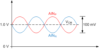
NOTE
Remember, common-mode voltage requirements with PGA enabled (Equation 13 to Equation 15) are as follows:
- VCM (MIN) ≥ AVSS + ¼ (AVDD – AVSS)
- VCM (MIN) ≥ AVSS + 0.2 V + ½ Gain · VIN (MAX)
- VCM (MAX) ≤ AVDD – 0.2 V – ½ Gain · VIN (MAX)
8.3.2.2 Bypassing the PGA
At gains of 1, 2, and 4, the device can be configured to disable and bypass the low-noise PGA by setting the PGA_BYPASS bit in the configuration register. Disabling the PGA lowers the overall power consumption and also removes the restrictions of Equation 13 through Equation 15 for the common-mode input voltage range, VCM. The usable absolute and common-mode input voltage range is (AVSS – 0.1 V ≤ V(AINx), VCM ≤ AVDD + 0.1 V) when the PGA is disabled.
In order to measure single-ended signals that are referenced to AVSS (AINP = VIN, AINN = AVSS), the PGA must be bypassed. Configure the device for single-ended measurements by either connecting one of the analog inputs to AVSS externally or by using the internal AVSS connection of the multiplexer (MUX[3:0] settings 1000 through 1011). When configuring the internal multiplexer for settings where AINN = AVSS (MUX[3:0] = 1000 through 1011) the PGA is automatically bypassed and disabled irrespective of the PGA_BYPASS setting and gain is limited to 1, 2, and 4. In case gain is set to greater than 4, the device limits gain to 4.
When the PGA is disabled, the device uses a buffered switched-capacitor stage to obtain gains of 1, 2, and 4. An internal buffer in front of the switched-capacitor stage ensures that the effect on the input loading resulting from the capacitor charging and discharging is minimal. See Figure 21 to Figure 26 for the typical values of absolute input currents (current flowing into or out of each input) and differential input currents (difference in absolute current between positive and negative input) when the PGA is disabled.
For signal sources with high output impedance, external buffering may still be necessary. Note that active buffers introduce noise and also introduce offset and gain errors. Consider all of these factors in high-accuracy applications.
8.3.3 Modulator
A ΔΣ modulator is used in the ADS1120 to convert the analog input voltage into a pulse code modulated (PCM) data stream. The modulator runs at a modulator clock frequency of f(MOD) = f(CLK) / 16 in normal and duty-cycle mode and f(MOD) = f(CLK) / 8 in turbo mode, where f(CLK) is either provided by the internal oscillator or the external clock source. Table 10 shows the modulator frequency for each operating mode using either the internal oscillator or an external clock of 4.096 MHz.
Table 10. Modulator Clock Frequency for Different Operating Modes(1)
| OPERATING MODE | f(MOD) |
|---|---|
| Duty-cycle mode | 256 kHz |
| Normal mode | 256 kHz |
| Turbo mode | 512 kHz |
8.3.4 Digital Filter
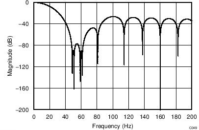
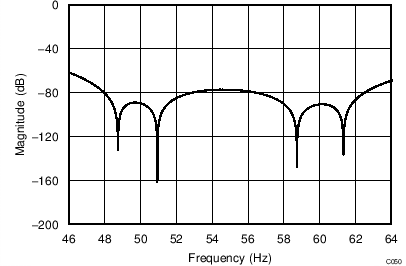
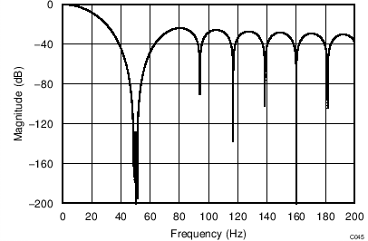
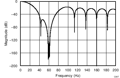
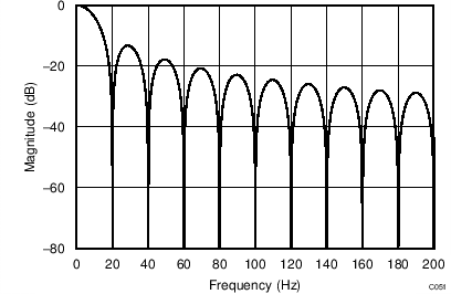
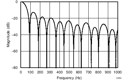
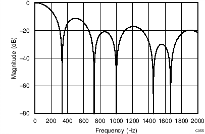
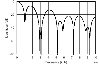
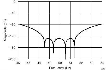
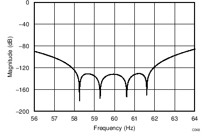
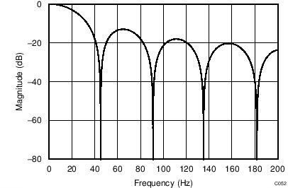
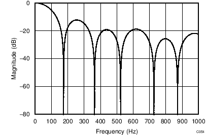
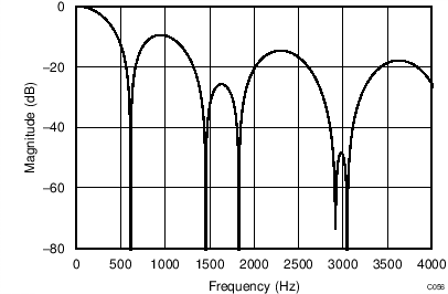
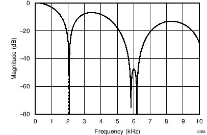
The device uses a linear-phase finite impulse response (FIR) digital filter that performs both filtering and decimation of the digital data stream coming from the modulator. The digital filter is automatically adjusted for the different data rates and always settles within a single cycle. At data rates of 5 SPS and 20 SPS, the filter can be configured to reject 50-Hz or 60-Hz line frequencies or to simultaneously reject 50 Hz and 60 Hz. Two bits (50/60[1:0]) in the configuration register are used to configure the filter accordingly. The frequency responses of the digital filter are shown in Figure 46 to Figure 59 for different output data rates using the internal oscillator or an external 4.096-MHz clock.
The filter notches and output data rate scale proportionally with the clock frequency. For example, a notch that appears at 20 Hz when using a 4.096-MHz clock appears at 10 Hz if a 2.048-MHz clock is used. Note that the internal oscillator can vary over temperature as specified in the Electrical Characteristics table. The data rate or conversion time, respectively, and filter notches consequently vary by the same amount. Consider using an external precision clock source if a digital filter notch at a specific frequency with a tighter tolerance is required.
| Simultaneous 50-Hz and 60-Hz Rejection, 50/60[1:0] = 01 |
(DR = 20 SPS)
| Simultaneous 50-Hz and 60-Hz Rejection, 50/60[1:0] = 01 |
(DR = 20 SPS)
| 50-Hz Rejection Only, 50/60[1:0] = 10 |
(DR = 20 SPS)
| 60-Hz Rejection Only, 50/60[1:0] = 11 |
(DR = 20 SPS)
| 50/60[1:0] = 00 |
(DR = 20 SPS)
(DR = 90 SPS)
(DR = 330 SPS)
(DR = 1 kSPS)
| 50-Hz Rejection Only, 50/60[1:0] = 10 |
(DR = 20 SPS)
| 60-Hz Rejection Only, 50/60[1:0] = 11 |
(DR = 20 SPS)
(DR = 45 SPS)
(DR = 175 SPS)
(DR = 600 SPS)
(DR = 2 kSPS)
8.3.5 Output Data Rate
Table 11 shows the actual conversion times for each data rate setting. The values provided are in terms of t(CLK) cycles using an external clock with a clock frequency of f(CLK) = 4.096 MHz. The data rates scale proportionally in case an external clock with a frequency other than 4.096 MHz is used.
Continuous conversion mode data rates are timed from one DRDY falling edge to the next DRDY falling edge. The first conversion starts 210 · t(CLK) (normal mode, duty-cycle mode) or 114 · t(CLK) (turbo mode) after the last SCLK falling edge of the START/SYNC command.
Single-shot mode data rates are timed from the last SCLK falling edge of the START/SYNC command to the DRDY falling edge and rounded to the next t(CLK). In case the internal oscillator is used, an additional oscillator wake-up time of up to 50 µs (normal mode, duty-cycle mode) or 25 µs (turbo mode) must be added in single-shot mode. The internal oscillator starts to power up at the first SCLK rising edge of the START/SYNC command. If an SCLK frequency higher than 160 kHz (normal mode, duty-cycle mode) or 320 kHz (turbo mode) is used, the oscillator may not be fully powered up at the end of the START/SYNC command. The ADC then waits until the internal oscillator is fully powered up before starting a conversion.
Single-shot conversion times in duty-cycle mode are the same as in normal mode. See the Duty-Cycle Mode section for more details on duty-cycle mode operation.
Table 11. Conversion Times
| NOMINAL DATA RATE (SPS) |
–3-dB BANDWIDTH (Hz) |
ACTUAL CONVERSION TIME (t(CLK)) | |
|---|---|---|---|
| CONTINUOUS CONVERSION MODE | SINGLE-SHOT MODE | ||
| Normal Mode | |||
| 20 | 13.1 | 204768 | 204850 |
| 45 | 20.0 | 91120 | 91218 |
| 90 | 39.6 | 46128 | 46226 |
| 175 | 77.8 | 23664 | 23762 |
| 330 | 150.1 | 12464 | 12562 |
| 600 | 279.0 | 6896 | 6994 |
| 1000 | 483.8 | 4144 | 4242 |
| Duty-Cycle Mode | |||
| 5 | 13.1 | 823120 | n/a |
| 11.25 | 20.0 | 364560 | n/a |
| 22.5 | 39.6 | 184592 | n/a |
| 44 | 77.8 | 94736 | n/a |
| 82.5 | 150.1 | 49936 | n/a |
| 150 | 279.0 | 27664 | n/a |
| 250 | 483.8 | 16656 | n/a |
| Turbo Mode | |||
| 40 | 26.2 | 102384 | 102434 |
| 90 | 39.9 | 45560 | 45618 |
| 180 | 79.2 | 23064 | 23122 |
| 350 | 155.6 | 11832 | 11890 |
| 660 | 300.3 | 6232 | 6290 |
| 1200 | 558.1 | 3448 | 3506 |
| 2000 | 967.6 | 2072 | 2130 |
Note that even though the conversion time at the 20-SPS setting is not exactly 1 / 20 Hz = 50 ms, this discrepancy does not affect the 50-Hz or 60-Hz rejection. To achieve the 50-Hz and 60-Hz rejection specified in the Electrical Characteristics, the external clock frequency must be 4.096 MHz. When using the internal oscillator, the conversion time and filter notches vary by the amount specified in the Electrical Characteristics table for oscillator accuracy.
8.3.6 Voltage Reference
The device offers an integrated low-drift, 2.048-V reference. For applications that require a different reference voltage value or a ratiometric measurement approach, the device offers two differential reference input pairs (REFP0, REFN0 and REFP1, REFN1). In addition, the analog supply (AVDD – AVSS) can be used as a reference.
The reference source is selected by two bits (VREF[1:0]) in the configuration register. By default, the internal reference is selected. The internal voltage reference requires less than 25 µs to fully settle after power-up, when coming out of power-down mode, or when switching from an external reference source to the internal reference.
The differential reference inputs allow freedom in the reference common-mode voltage. REFP0 and REFN0 are dedicated reference inputs whereas REFP1 and REFN1 are shared with inputs AIN0 and AIN3, respectively. All reference inputs are internally buffered to increase input impedance. Therefore, additional reference buffers are usually not required when using an external reference. When used in ratiometric applications, the reference inputs do not load the external circuitry. Note that the analog supply current increases when using an external reference because the reference buffers are enabled.
In most cases the conversion result is directly proportional to the stability of the reference source. Any noise and drift of the voltage reference is reflected in the conversion result.
8.3.7 Clock Source
The device system clock can either be provided by the internal low-drift oscillator or by an external clock source on the CLK input. Connect the CLK pin to DGND before power-up or reset to activate the internal oscillator. Connecting an external clock to the CLK pin at any time deactivates the internal oscillator after two rising edges on the CLK pin are detected. The device then operates on the external clock. After the ADS1120 switches to the external clock, the device can only be switched back to the internal oscillator by cycling the power supplies or by sending a RESET command.
8.3.8 Excitation Current Sources
The device provides two matched programmable excitation current sources (IDACs) for RTD applications. The output current of the current sources can be programmed to 50 μA, 100 μA, 250 μA, 500 μA, 1000 μA, or 1500 μA using the respective bits (IDAC[2:0]) in the configuration register. Each current source can be connected to any of the analog inputs (AINx) as well as to any of the dedicated reference inputs (REFP0 and REFN0). Both current sources can also be connected to the same pin. Routing of the IDACs is configured by bits (I1MUX[2:0], I2MUX[2:0]) in the configuration register. Care must be taken not to exceed the compliance voltage of the IDACs. In other words, limit the voltage on the pin where the IDAC is routed to ≤ (AVDD – 0.9 V), otherwise the specified accuracy of the IDAC current is not met. For three-wire RTD applications, the matched current sources can be used to cancel errors caused by sensor lead resistance (see the 3-Wire RTD Measurement section for more details).
The IDACs require up to 200 µs to start up after the IDAC current is programmed to the respective value using bits IDAC[2:0]. If configuration registers 2 and 3 are not written during the same WREG command, TI recommends to first set the IDAC current to the respective value using bits IDAC[2:0] and thereafter select the routing for each IDAC (I1MUX[2:0], I2MUX[2:0]).
In single-shot mode, the IDACs remain active between any two conversions if the IDAC[2:0] bits are set to a value other than 000. However, the IDACs are powered down whenever the POWERDOWN command is issued.
Note that the analog supply current increases when enabling the IDACs (that is, when the IDAC[2:0] bits are set to a value other than 000). The IDAC circuit needs this bias current to operate even when the IDACs are not routed to any pin (I1MUX[2:0] = I2MUX[2:0] = 000). In addition, the selected output current is drawn from the analog supply when I1MUX[2:0] or I2MUX[2:0] are set to a value other than 000.
8.3.9 Low-Side Power Switch
A low-side power switch with low on-resistance connected between the analog input AIN3/REFN1 and AVSS is integrated in the device as well. This power switch can be used to reduce system power consumption in bridge sensor applications by powering down the bridge circuit between conversions. When the respective bit (PSW) in the configuration register is set, the switch automatically closes when the START/SYNC command is sent and opens when the POWERDOWN command is issued. Note that the switch stays closed between conversions in single-shot mode in case the PSW bit is set to 1. The switch can be opened at any time by setting the PSW bit to 0. By default, the switch is always open.
8.3.10 Sensor Detection
To help detect a possible sensor malfunction, the device provides internal 10-µA, burn-out current sources. When enabled by setting the respective bit (BCS) in the configuration register, one current source sources current to the positive analog input (AINP) currently selected while the other current source sinks current form the selected negative analog input (AINN).
In case of an open circuit in the sensor, these burn-out current sources pull the positive input towards AVDD and the negative input towards AVSS, resulting in a full-scale reading. A full-scale reading may also indicate that the sensor is overloaded or that the reference voltage is absent. A near-zero reading may indicate a shorted sensor. Note that the absolute value of the burn-out current sources typically varies by ±10% and the internal multiplexer adds a small series resistance. Therefore, distinguishing a shorted sensor condition from a normal reading can be difficult, especially if an RC filter is used at the inputs. In other words, even if the sensor is shorted, the voltage drop across the external filter resistance and the residual resistance of the multiplexer causes the output to read a value higher than zero.
Keep in mind that ADC readings of a functional sensor may be corrupted when the burn-out current sources are enabled. TI recommends disabling the burn-out current sources when preforming the precision measurement, and only enabling them to test for sensor fault conditions.
8.3.11 System Monitor
The device provides some means for monitoring the analog power supply and the external voltage reference. To select a monitoring voltage, the internal multiplexer (MUX[3:0]) must be configured accordingly in the configuration register. The device automatically bypasses the PGA and sets the gain to 1, irrespective of the configuration register settings while the monitoring feature is used. Note that the system monitor function only provides a coarse result and is not meant to be a precision measurement.
When measuring the analog power supply (MUX[3:0] = 1101), the resulting conversion is approximately (AVDD – AVSS) / 4. The device uses the internal 2.048-V reference for the measurement regardless of what reference source is selected in the configuration register (VREF[1:0]).
When monitoring one of the two possible external reference voltage sources (MUX[3:0] = 1100), the result is approximately (V(REFPx) – V(REFNx)) / 4. REFPx and REFNx denote the external reference input pair selected in the configuration register (VREF[1:0]). The device automatically uses the internal reference for the measurement.
8.3.12 Offset Calibration
The internal multiplexer offers the option to short both PGA inputs (AINP and AINN) to mid-supply (AVDD + AVSS) / 2. This option can be used to measure and calibrate the device offset voltage by storing the result of the shorted input voltage reading in a microcontroller and consequently subtracting the result from each following reading. TI recommends taking multiple readings with the inputs shorted and averaging the result to reduce the effect of noise.
8.3.13 Temperature Sensor
The ADS1120 offers an integrated precision temperature sensor. The temperature sensor mode is enabled by setting bit TS = 1 in the configuration register. When in temperature sensor mode, the settings of configuration register 0 have no effect and the device uses the internal reference for measurement, regardless of the selected voltage reference source. Temperature readings follow the same process as the analog inputs for starting and reading conversion results. Temperature data are represented as a 14-bit result that is left-justified within the 16-bit conversion result. Data are output starting with the most significant byte (MSB). When reading the two data bytes, the first 14 bits are used to indicate the temperature measurement result. One 14-bit LSB equals 0.03125°C. Negative numbers are represented in binary twos complement format, as shown in Table 12.
Table 12. 14-Bit Temperature Data Format
| TEMPERATURE (°C) | DIGITAL OUTPUT | |
|---|---|---|
| BINARY | HEX | |
| 128 | 01 0000 0000 0000 | 1000 |
| 127.96875 | 00 1111 1111 1111 | 0FFF |
| 100 | 00 1100 1000 0000 | 0C80 |
| 75 | 00 1001 0110 0000 | 0960 |
| 50 | 00 0110 0100 0000 | 0640 |
| 25 | 00 0011 0010 0000 | 0320 |
| 0.25 | 00 0000 0000 1000 | 0008 |
| 0.03125 | 00 0000 0000 0001 | 0001 |
| 0 | 00 0000 0000 0000 | 0000 |
| –0.25 | 11 1111 1111 1000 | 3FF8 |
| –25 | 11 1100 1110 0000 | 3CE0 |
| –55 | 11 1001 0010 0000 | 3920 |
8.3.13.1 Converting from Temperature to Digital Codes
8.3.13.1.1 For Positive Temperatures (for Example, 50°C):
Twos complement is not performed on positive numbers. Therefore, simply convert the number to binary code in a 14-bit, left-justified format with the MSB = 0 to denote the positive sign.
Example: 50°C / (0.03125°C per count) = 1600 = 0640h = 00 0110 0100 0000
8.3.13.1.2 For Negative Temperatures (for Example, –25°C):
Generate the twos complement of a negative number by complementing the absolute binary number and adding 1. Then, denote the negative sign with the MSB = 1.
Example: |–25°C| / (0.03125°C per count) = 800 = 0320h = 00 0011 0010 0000
Twos complement format: 11 1100 1101 1111 + 1 = 11 1100 1110 0000
8.3.13.2 Converting from Digital Codes to Temperature
To convert from digital codes to temperature, first check whether the MSB is a 0 or a 1. If the MSB is a 0, simply multiply the decimal code by 0.03125°C to obtain the result. If the MSB = 1, subtract 1 from the result and complement all bits. Then, multiply the result by –0.03125°C.
Example: The device reads back 0960h: 0960h has an MSB = 0.
0960h · 0.03125°C = 2400 · 0.03125°C = 75°C
Example: The device reads back 3CE0h: 3CE0h has an MSB = 1.
Subtract 1 and complement the result: 3CE0h → 0320h
0320h · (–0.03125°C) = 800 · (–0.03125°C) = –25°C
8.4 Device Functional Modes
8.4.1 Power-Up and Reset
When the device powers up, a reset is performed. The reset process takes approximately 50 µs. After this power-up reset time, all internal circuitry (including the voltage reference) are stable and communication with the device is possible. As part of the reset process, the device sets all bits in the configuration registers to the respective default settings. By default, the device is set to single-shot mode. After power-up, the device performs a single conversion using the default register settings and then enters a low-power state. When the conversion is complete, the DRDY pin transitions from high to low. The high-to-low transition of the DRDY pin can be used to signal that the ADS1120 is operational and ready to use. The power-up behavior is intended to prevent systems with tight power-supply requirements from encountering a current surge during power-up.
8.4.2 Conversion Modes
The device can be operated in one of two conversion modes that can be selected by the CM bit in the configuration register. These conversion modes are single-shot and continuous conversion mode.
8.4.2.1 Single-Shot Mode
In single-shot mode, the device only performs a conversion when a START/SYNC command is issued. The device consequently performs one single conversion and returns to a low-power state afterwards. The internal oscillator and all analog circuitry (except for the excitation current sources) are turned off while the device waits in this low-power state until the next conversion is started. In addition, every write access to any configuration register also starts a new conversion. Writing to any configuration register while a conversion is ongoing functions as a new START/SYNC command that stops the current conversion and restarts a single new conversion. Each conversion is fully settled (assuming the analog input signal settles to its final value before the conversion starts) because the device digital filter settles within a single cycle.
8.4.2.2 Continuous Conversion Mode
In continuous conversion mode, the device continuously performs conversions. When a conversion completes, the device places the result in the output buffer and immediately begins another conversion.
In order to start continuous conversion mode, the CM bit must be set to 1 followed by a START/SYNC command. The first conversion starts 210 · t(CLK) (normal mode, duty-cycle mode) or 114 · t(CLK) (turbo mode) after the last SCLK falling edge of the START/SYNC command. Writing to any configuration register during an ongoing conversion restarts the current conversion. TI recommends always sending a START/SYNC command immediately after the CM bit is set to 1.
8.4.3 Operating Modes
In addition to the different conversion modes, the device can also be operated in different operating modes that can be selected to trade-off power consumption, noise performance, and output data rate. These modes are: normal mode, duty-cycle mode, turbo mode, and power-down mode.
8.4.3.1 Normal Mode
Normal mode is the default mode of operation after power-up. In this mode, the internal modulator of the ΔΣ ADC runs at a modulator clock frequency of f(MOD) = f(CLK) / 16, where the system clock (f(CLK)) is either provided by the internal oscillator or the external clock source. The modulator frequency is 256 kHz when using the internal oscillator. Normal mode offers output data rate options ranging from 20 SPS to 1 kSPS with the internal oscillator. The data rate is selected by the DR[2:0] bits in the configuration register. In case an external clock source with a clock frequency other than 4.096 MHz is used, the data rates scale accordingly. For example, using an external clock with f(CLK) = 2.048 MHz yields data rates ranging from 10 SPS to 500 SPS.
8.4.3.2 Duty-Cycle Mode
The noise performance of a ΔΣ ADC generally improves when lowering the output data rate because more samples of the internal modulator can be averaged to yield one conversion result. In applications where power consumption is critical, the improved noise performance at low data rates may not be required. For these applications, the device supports an automatic duty-cycle mode that can yield significant power savings by periodically entering a low-power state between conversions. In principle, the device runs in normal mode with a duty cycle of 25%. This functionality means the device performs one conversion in the same manner as when running in normal mode but then automatically enters a low power-state for three consecutive conversion cycles. The noise performance in duty-cycle mode is therefore comparable to the noise performance in normal mode at four times the data rate. Data rates in duty-cycle mode range from 5 SPS to 250 SPS with the internal oscillator.
8.4.3.3 Turbo Mode
Applications that require higher data rates up to 2 kSPS can operate the device in turbo mode. In this mode, the internal modulator runs at a higher frequency of f(MOD) = f(CLK) / 8. f(MOD) equals 512 kHz when the internal oscillator or an external 4.096-MHz clock is used. Note that the device power consumption increases because the modulator runs at a higher frequency. Running the ADS1120 in turbo mode at a comparable output data rate as in normal mode yields better noise performance. For example, the input-referred noise at 90 SPS in turbo mode is lower than the input-referred noise at 90 SPS in normal mode.
8.4.3.4 Power-Down Mode
When the POWERDOWN command is issued, the device enters power-down mode after completing the current conversion. In this mode, all analog circuitry (including the voltage reference and both IDACs) are powered down, the low-side power switch is opened, and the device typically only uses 400 nA of current. While in power-down mode, the device holds the configuration register settings and responds to commands, but does not perform any data conversions.
Issuing a START/SYNC command wakes up the device and either starts a single conversion or starts continuous conversion mode, depending on the conversion mode selected by the CM bit. Note that writing to any configuration register wakes up the device as well, but only starts a single conversion regardless of the selected conversion mode (CM).
8.5 Programming
8.5.1 Serial Interface
The SPI-compatible serial interface of the device is used to read conversion data, read and write the device configuration registers, and control device operation. Only SPI mode 1 (CPOL = 0, CPHA = 1) is supported. The interface consists of five control lines (CS, SCLK, DIN, DOUT/DRDY, and DRDY) but can be used with only four or even three control signals as well. The dedicated data-ready signal (DRDY) can be configured to be shared with DOUT/DRDY. If the serial bus is not shared with any other device, CS can be tied low permanently so that only signals SCLK, DIN, and DOUT/DRDY are required to communicate with the device.
8.5.1.1 Chip Select (CS)
Chip select (CS) is an active-low input that selects the device for SPI communication. This feature is useful when multiple devices share the same serial bus. CS must remain low for the duration of the serial communication. When CS is taken high, the serial interface is reset, SCLK is ignored, and DOUT/DRDY enters a high-impedance state; as such, DOUT/DRDY cannot indicate when data are ready. In situations where multiple devices are present on the bus, the dedicated DRDY pin can provide an uninterrupted monitor of the conversion status. If the serial bus is not shared with another peripheral, CS can be tied low.
8.5.1.2 Serial Clock (SCLK)
The serial clock (SCLK) features a Schmitt-triggered input and is used to clock data into and out of the device on the DIN and DOUT/DRDY pins, respectively. Even though the input has hysteresis, TI recommends keeping the SCLK signal as clean as possible to prevent glitches from accidentally shifting the data. When the serial interface is idle, hold SCLK low.
8.5.1.3 Data Ready (DRDY)
DRDY indicates when a new conversion result is ready for retrieval. When DRDY falls low, new conversion data are ready. DRDY transitions back high on the next SCLK rising edge. When no data are read during continuous conversion mode, DRDY remains low but pulses high for a duration of 2 · t(MOD) prior to the next DRDY falling edge. The DRDY pin is always actively driven, even when CS is high.
8.5.1.4 Data Input (DIN)
The data input pin (DIN) is used along with SCLK to send data (commands and register data) to the device. The device latches data on DIN on the SCLK falling edge. The device never drives the DIN pin.
8.5.1.5 Data Output and Data Ready (DOUT/DRDY)
DOUT/DRDY serves a dual-purpose function. This pin is used with SCLK to read conversion and register data from the device. Data on DOUT/DRDY are shifted out on the SCLK rising edge. DOUT/DRDY goes to a high-impedance state when CS is high.
In addition, the DOUT/DRDY pin can also be configured as a data-ready indicator by setting the DRDYM bit high in the configuration register. DOUT/DRDY then transitions low at the same time that the DRDY pin goes low to indicate new conversion data are available. Both signals can be used to detect if new data are ready. However, because DOUT/DRDY is disabled when CS is high, the recommended method of monitoring the end of a conversion when multiple devices are present on the SPI bus is to use the dedicated DRDY pin.
8.5.1.6 SPI Timeout
The ADS1120 offers an SPI timeout feature that can be used to recover communication when a serial interface transmission is interrupted. This feature is especially useful in applications where CS is permanently tied low and is not used to frame a communication sequence. Whenever a complete command is not sent within 13955 · t(MOD) (normal mode, duty-cycle mode) or 27910 · t(MOD) (turbo mode), the serial interface resets and the next SCLK pulse starts a new communication cycle. See the Modulator section for details on the modulator frequency (f(MOD) = 1 / t(MOD)) in the different operating modes. For the RREG and WREG commands, a complete command includes the command byte itself plus the register bytes that are read or written.
8.5.2 Data Format
The device provides 16 bits of data in binary twos complement format. The size of one code (LSB) is calculated using Equation 16.
A positive full-scale input [VIN ≥ (+FS – 1 LSB) = (Vref / Gain – 1 LSB)] produces an output code of 7FFFh and a negative full-scale input (VIN ≤ –FS = –Vref / Gain) produces an output code of 8000h. The output clips at these codes for signals that exceed full-scale.
Table 13 summarizes the ideal output codes for different input signals.
Table 13. Ideal Output Code versus Input Signal
| INPUT SIGNAL VIN = (V(AINP) – V(AINN)) |
IDEAL OUTPUT CODE(1) |
|---|---|
| ≥ +FS (215 – 1) / 215 | 7FFFh |
| +FS / 215 | 0001h |
| 0 | 0000h |
| –FS / 215 | FFFFh |
| ≤ –FS | 8000h |
Mapping of the analog input signal to the output codes is shown in Figure 60.
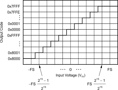 Figure 60. Code Transition Diagram
8.5.3 Commands
The device offers six different commands to control device operation, as shown in Table 14. Four commands are stand-alone instructions (RESET, START/SYNC, POWERDOWN, and RDATA). The commands to read (RREG) and write (WREG) configuration register data from and to the device require additional information as part of the instruction.
Table 14. Command Definitions
| COMMAND | DESCRIPTION | COMMAND BYTE(1) |
|---|---|---|
| RESET | Reset the device | 0000 011x |
| START/SYNC | Start or restart conversions | 0000 100x |
| POWERDOWN | Enter power-down mode | 0000 001x |
| RDATA | Read data by command | 0001 xxxx |
| RREG | Read nn registers starting at address rr | 0010 rrnn |
| WREG | Write nn registers starting at address rr | 0100 rrnn |
8.5.3.1 RESET (0000 011x)
Resets the device to the default values. Wait at least (50 µs + 32 · t(CLK)) after the RESET command is sent before sending any other command.
8.5.3.2 START/SYNC (0000 100x)
In single-shot mode, the START/SYNC command is used to start a single conversion, or (when sent during an ongoing conversion) to reset the digital filter, and then restarts a single new conversion. When the device is set to continuous conversion mode, the START/SYNC command must be issued one time to start converting continuously. Sending the START/SYNC command while converting in continuous conversion mode resets the digital filter and restarts continuous conversions.
8.5.3.3 POWERDOWN (0000 001x)
The POWERDOWN command places the device into power-down mode. This command shuts down all internal analog components, opens the low-side switch, turns off both IDACs, but holds all register values. In case the POWERDOWN command is issued while a conversion is ongoing, the conversion completes before the ADS1120 enters power-down mode. As soon as a START/SYNC command is issued, all analog components return to their previous states.
8.5.3.4 RDATA (0001 xxxx)
The RDATA command loads the output shift register with the most recent conversion result. This command can be used when DOUT/DRDY or DRDY are not monitored to indicate that a new conversion result is available. If a conversion finishes in the middle of the RDATA command byte, the state of the DRDY pin at the end of the read operation signals whether the old or the new result is loaded. If the old result is loaded, DRDY stays low, indicating that the new result is not read out. The new conversion result loads when DRDY is high.
8.5.3.5 RREG (0010 rrnn)
The RREG command reads the number of bytes specified by nn (number of bytes to be read – 1) from the device configuration register, starting at register address rr. The command is completed after nn + 1 bytes are clocked out after the RREG command byte. For example, the command to read three bytes (nn = 10) starting at configuration register 1 (rr = 01) is 0010 0110.
8.5.3.6 WREG (0100 rrnn)
The WREG command writes the number of bytes specified by nn (number of bytes to be written – 1) to the device configuration register, starting at register address rr. The command is completed after nn + 1 bytes are clocked in after the WREG command byte. For example, the command to write two bytes (nn = 01) starting at configuration register 0 (rr = 00) is 0100 0001. The configuration registers are updated on the last SCLK falling edge.
8.5.4 Reading Data
Output pins DRDY and DOUT/DRDY (if the DRDYM bit is set high in the configuration register) transition low when new data are ready for retrieval. The conversion data are written to an internal data buffer. Data can be read directly from this buffer on DOUT/DRDY when DRDY falls low without concern of data corruption. An RDATA command does not have to be sent. Data are shifted out on the SCLK rising edges, MSB first, and consist of two bytes of data.
Figure 61 to Figure 63 show the timing diagrams for reading conversion data in continuous conversion mode and single-shot mode when not using the RDATA command.
 Figure 61. Continuous Conversion Mode (DRDYM = 0)
 Figure 62. Continuous Conversion Mode (DRDYM = 1)
 Figure 63. Single-Shot Mode (DRDYM = 0)
Data can also be read at any time without synchronizing to the DRDY signal using the RDATA command. When an RDATA command is issued, the conversion result currently stored in the data buffer is shifted out on DOUT/DRDY on the following SCLK rising edges. Data can be read continuously with the RDATA command as an alternative to monitoring DRDY or DOUT/DRDY. The DRDY pin can be polled after the LSB is clocked out to determine if a new conversion result was loaded. If a new conversion completes during the read operation but data from the previous conversion are read, then DRDY is low. Otherwise, if the most recent result is read, DRDY is high. Figure 64 and Figure 65 illustrate the behavior for both cases.
 Figure 64. State of DRDY when a New Conversion Finishes During an RDATA Command
 Figure 65. State of DRDY when the Most Recent Conversion Result is Read During an RDATA Command
8.5.5 Sending Commands
The device serial interface is capable of full-duplex operation while reading conversion data when not using the RDATA command. Full-duplex operation means commands are decoded at the same time that conversion data are read. Commands can be sent on any 8-bit data boundary during a data read operation. When a RREG or RDATA command is recognized, the current data read operation is aborted and the conversion data are corrupted, unless the command is sent while the last byte of the conversion result is retrieved. The device starts to output the requested data on DOUT/DRDY at the first SCLK rising edge after the command byte. To read data without interruption, keep DIN low while clocking out data.
A WREG command can be sent without corrupting an ongoing read operation. Figure 66 shows an example for sending a WREG command to write two configuration registers while reading conversion data in continuous conversion mode. After the command is clocked in (after the 32nd SCLK falling edge), the device resets the digital filter and starts converting with the new register settings. The WREG command can be sent on any of the 8-bit boundaries.
 Figure 66. Example of Reading Data while Simultaneously Sending a WREG Command
Note that the serial interface does not decode commands while an RDATA or RREG command is executed. That is, all 16 bits of the conversion result must be read after the RDATA command is issued and all requested registers must be read after a RREG command is sent before a new command can be issued.
8.5.6 Interfacing with Multiple Devices
When connecting multiple ADS1120 devices to a single SPI bus, SCLK, DIN, and DOUT/DRDY can be safely shared by using a dedicated chip-select (CS) line for each SPI-enabled device. When CS transitions high for the respective device, DOUT/DRDY enters a 3-state mode. Therefore, DOUT/DRDY cannot be used to indicate when new data are available if CS is high, regardless of the DRDYM bit setting in the configuration register. Only the dedicated DRDY pin indicates that new data are available, because the DRDY pin is actively driven even when CS is high.
In some cases the DRDY pin cannot be interfaced to the microcontroller. This scenario can occur if there are insufficient GPIO channels available on the microcontroller or if the serial interface must be galvanically isolated and thus the amount of channels must be limited. Therefore, in order to evaluate when a new conversion of one of the devices is ready, the microcontroller can periodically drop CS to the respective device and poll the state of the DOUT/DRDY pin. When CS goes low, the DOUT/DRDY pin immediately drives either high or low, provided that the DRDYM bit is configured to 1. If the DOUT/DRDY line drives low, when CS is taken low, new data are currently available. If the DOUT/DRDY line drives high, no new data are available. This procedure requires that DOUT/DRDY is high after reading each conversion result and before taking CS high. To make sure DOUT/DRDY is taken high, send 16 additional SCLKs with DIN held low after each data read operation. DOUT/DRDY reads low during the first eight SCLKs after the conversion result is read, and reads high during the following eight SCLKs, as shown in Figure 67. Alternatively, valid data can be retrieved from the device at any time without concern of data corruption by using the RDATA command.
 Figure 67. Example of Taking DOUT/DRDY High After Reading a Conversion Result
8.6 Register Map
8.6.1 Configuration Registers
The device has four 8-bit configuration registers that are accessible through the serial interface using the RREG and WREG commands. The configuration registers control how the device operates and can be changed at any time without causing data corruption. After power-up or reset, all registers are set to the default values (which are all 0). All registers retain their values during power-down mode. Table 15 shows the register map of the configuration registers.
Table 15. Configuration Register Map
8.6.1.1 Configuration Register 0 (offset = 00h) [reset = 00h]
| 7 | 6 | 5 | 4 | 3 | 2 | 1 | 0 |
| MUX[3:0] | GAIN[2:0] | PGA_BYPASS | |||||
| R/W-0h | R/W-0h | R/W-0h | |||||
| LEGEND: R/W = Read/Write; -n = value after reset |
Table 16. Configuration Register 0 Field Descriptions
| Bit | Field | Type | Reset | Description |
|---|---|---|---|---|
| 7:4 | MUX[3:0] | R/W | 0h | Input multiplexer configuration
These bits configure the input multiplexer. For settings where AINN = AVSS, the PGA must be disabled (PGA_BYPASS = 1) and only gains 1, 2, and 4 can be used. 0000 : AINP = AIN0, AINN = AIN1 (default) 0001 : AINP = AIN0, AINN = AIN2 0010 : AINP = AIN0, AINN = AIN3 0011 : AINP = AIN1, AINN = AIN2 0100 : AINP = AIN1, AINN = AIN3 0101 : AINP = AIN2, AINN = AIN3 0110 : AINP = AIN1, AINN = AIN0 0111 : AINP = AIN3, AINN = AIN2 1000 : AINP = AIN0, AINN = AVSS 1001 : AINP = AIN1, AINN = AVSS 1010 : AINP = AIN2, AINN = AVSS 1011 : AINP = AIN3, AINN = AVSS 1100 : (V(REFPx) – V(REFNx)) / 4 monitor (PGA bypassed) 1101 : (AVDD – AVSS) / 4 monitor (PGA bypassed) 1110 : AINP and AINN shorted to (AVDD + AVSS) / 2 1111 : Reserved |
| 3:1 | GAIN[2:0] | R/W | 0h | Gain configuration
These bits configure the device gain. Gains 1, 2, and 4 can be used without the PGA. In this case, gain is obtained by a switched-capacitor structure. 000 : Gain = 1 (default) 001 : Gain = 2 010 : Gain = 4 011 : Gain = 8 100 : Gain = 16 101 : Gain = 32 110 : Gain = 64 111 : Gain = 128 |
| 0 | PGA_BYPASS | R/W | 0h | Disables and bypasses the internal low-noise PGA
Disabling the PGA reduces overall power consumption and allows the common-mode voltage range (VCM) to span from AVSS – 0.1 V to AVDD + 0.1 V. The PGA can only be disabled for gains 1, 2, and 4. The PGA is always enabled for gain settings 8 to 128, regardless of the PGA_BYPASS setting. 0 : PGA enabled (default) 1 : PGA disabled and bypassed |
8.6.1.2 Configuration Register 1 (offset = 01h) [reset = 00h]
| 7 | 6 | 5 | 4 | 3 | 2 | 1 | 0 |
| DR[2:0] | MODE[1:0] | CM | TS | BCS | |||
| R/W-0h | R/W-0h | R/W-0h | R/W-0h | R/W-0h | |||
| LEGEND: R/W = Read/Write; -n = value after reset |
Table 17. Configuration Register 1 Field Descriptions
| Bit | Field | Type | Reset | Description |
|---|---|---|---|---|
| 7:5 | DR[2:0] | R/W | 0h | Data rate
These bits control the data rate setting depending on the selected operating mode. Table 18 lists the bit settings for normal, duty-cycle, and turbo mode. |
| 4:3 | MODE[1:0] | R/W | 0h | Operating mode
These bits control the operating mode the device operates in. 00 : Normal mode (256-kHz modulator clock, default) 01 : Duty-cycle mode (internal duty cycle of 1:4) 10 : Turbo mode (512-kHz modulator clock) 11 : Reserved |
| 2 | CM | R/W | 0h | Conversion mode
This bit sets the conversion mode for the device. 0 : Single-shot mode (default) 1 : Continuous conversion mode |
| 1 | TS | R/W | 0h | Temperature sensor mode
This bit enables the internal temperature sensor and puts the device in temperature sensor mode. The settings of configuration register 0 have no effect and the device uses the internal reference for measurement when temperature sensor mode is enabled. 0 : Disables temperature sensor (default) 1 : Enables temperature sensor |
| 0 | BCS | R/W | 0h | Burn-out current sources
This bit controls the 10-µA, burn-out current sources. The burn-out current sources can be used to detect sensor faults such as wire breaks and shorted sensors. 0 : Current sources off (default) 1 : Current sources on |
Table 18. DR Bit Settings(1)
| NORMAL MODE | DUTY-CYCLE MODE | TURBO MODE |
|---|---|---|
| 000 = 20 SPS | 000 = 5 SPS | 000 = 40 SPS |
| 001 = 45 SPS | 001 = 11.25 SPS | 001 = 90 SPS |
| 010 = 90 SPS | 010 = 22.5 SPS | 010 = 180 SPS |
| 011 = 175 SPS | 011 = 44 SPS | 011 = 350 SPS |
| 100 = 330 SPS | 100 = 82.5 SPS | 100 = 660 SPS |
| 101 = 600 SPS | 101 = 150 SPS | 101 = 1200 SPS |
| 110 = 1000 SPS | 110 = 250 SPS | 110 = 2000 SPS |
| 111 = Reserved | 111 = Reserved | 111 = Reserved |
8.6.1.3 Configuration Register 2 (offset = 02h) [reset = 00h]
| 7 | 6 | 5 | 4 | 3 | 2 | 1 | 0 |
| VREF[1:0] | 50/60[1:0] | PSW | IDAC[2:0] | ||||
| R/W-0h | R/W-0h | R/W-0h | R/W-0h | ||||
| LEGEND: R/W = Read/Write; -n = value after reset |
Table 19. Configuration Register 2 Field Descriptions
8.6.1.4 Configuration Register 3 (offset = 03h) [reset = 00h]
| 7 | 6 | 5 | 4 | 3 | 2 | 1 | 0 |
| I1MUX[2:0] | I2MUX[2:0] | DRDYM | 0 | ||||
| R/W-0h | R/W-0h | R/W-0h | R/W-0h | ||||
| LEGEND: R/W = Read/Write; -n = value after reset |
Table 20. Configuration Register 3 Field Descriptions
| Bit | Field | Type | Reset | Description |
|---|---|---|---|---|
| 7:5 | I1MUX[2:0] | R/W | 0h | IDAC1 routing configuration
These bits select the channel where IDAC1 is routed to. 000 : IDAC1 disabled (default) 001 : IDAC1 connected to AIN0/REFP1 010 : IDAC1 connected to AIN1 011 : IDAC1 connected to AIN2 100 : IDAC1 connected to AIN3/REFN1 101 : IDAC1 connected to REFP0 110 : IDAC1 connected to REFN0 111 : Reserved |
| 4:2 | I2MUX[2:0] | R/W | 0h | IDAC2 routing configuration
These bits select the channel where IDAC2 is routed to. 000 : IDAC2 disabled (default) 001 : IDAC2 connected to AIN0/REFP1 010 : IDAC2 connected to AIN1 011 : IDAC2 connected to AIN2 100 : IDAC2 connected to AIN3/REFN1 101 : IDAC2 connected to REFP0 110 : IDAC2 connected to REFN0 111 : Reserved |
| 1 | DRDYM | R/W | 0h | DRDY mode
This bit controls the behavior of the DOUT/DRDY pin when new data are ready. 0 : Only the dedicated DRDY pin is used to indicate when data are ready (default) 1 : Data ready is indicated simultaneously on DOUT/DRDY and DRDY |
| 0 | Reserved | R/W | 0h | Reserved
Always write 0 |
