ZHCSDI9D January 2015 – January 2017 HD3SS460
PRODUCTION DATA.
9 Application and Implementation
NOTE
Information in the following applications sections is not part of the TI component specification, and TI does not warrant its accuracy or completeness. TI’s customers are responsible for determining suitability of components for their purposes. Customers should validate and test their design implementation to confirm system functionality.
9.1 Application Information
HD3SS460 can be utilized for a wide range of muxing needs. This is general purpose passive cross-point switch. The channels have independent adaptive common mode tracking allowing flexibility. As long as recommended electrical use conditions are met the device can be used number of ways as described in Table 1.
NOTE
HD3SS460 does not provide common mode biasing for the channel. Therefore it is required that the device is biased from either side for all active channels.
9.2 USB SS and DP as Alternate Mode
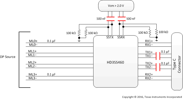
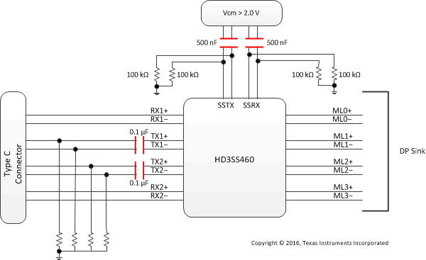
HD3SS460 can be used USB Type-C ecosystem with DP as alternate mode in two distinct application configurations – one is for DP Source/USB Host, the other one for the DP Sink/USB Device/Dock. Figure 3 and Figure 4 illustrate typical application block diagrams for these two cases. Detail schematics are illustrated in Detailed Design Procedure section. Other applications and or use cases possible where these examples can be used as general guidelines.
Figure 3 and Figure 4 depict the AC coupling capacitor placement examples. TI recommends placing the capacitors as shown in the illustrations for the backward compatibility and interoperability purposes as some of the existing USB systems may present Vcm, exceeding the typical range of 0–2 V on SS differential pairs.
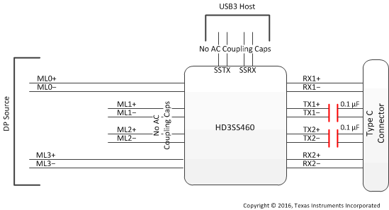 Figure 3. Block Diagram for a Type C Interface Using DP as Alternate Mode – Source/Host
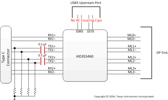 Figure 4. Diagram for a Type C Interface Using DP as Alternate Mode – Sink/Device/Dock
Figure 5 and Figure 6 depict the AC coupling capacitor recommendations in case the upstream or downstream port connected internally to the HD3SS460 presents Vcm greater than 2 V.
9.2.1 Design Requirements
| DESIGN PARAMETERS | EXAMPLE VALUES | |||
|---|---|---|---|---|
| VCC | 3.3 V | |||
| Decoupling capacitors | 0.1 µF | |||
| AC Capacitors | 75-200nF (100nF shown) USBSS TX p and n lines require AC capacotprs. Alternate mode signals may or may not require AC capacitors | |||
| Control pins | Controls pins can be dynamically controlled or pin-strapped. The POL signal is controlled by CC logic in the Type-C ecosystem. | |||
9.2.2 Detailed Design Procedure
The reference schematics shown in this document are based upon the pin assignment defined in the Alternate mode over Type C specification as shown in Figure 7 below.
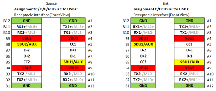 Figure 7. Pin Assignment – Alternate Mode Over Type C
Table 2 represents the example pin mapping to HD3SS460 for the DP Source pin assignments C, D, E and F, DP Sink pin assignments C and D.
Table 2. SOURCE Pin Assignment Option C and E (AMSEL = H, EN = H)
| RECEPTACLE PIN NUMBER | 460 PIN MAPPING TO TYPE C CONNECTOR | 460 PIN MAPPING TO DP SOURCE (GPU) | |
|---|---|---|---|
| POL = L | POL = H | ||
| A11/10 | CRX2 | LnA(ML0) | LnD(ML3) |
| A2/3 | CTX1 | LnC(ML2) | LnB(ML1) |
| B11/10 | CRX1 | LnD(ML3) | LnA(ML0) |
| B2/3 | CTX2 | LnB(ML1) | LnC(ML2) |
| A8 | CSBU1 | SBU1(AUXP) | SBU2(AUXN) |
| B8 | CSBU2 | SBU2(AUXN) | SBU1(AUXP) |
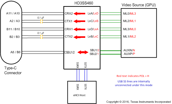 Figure 8. SOURCE Pin Assignment Option C and E (AMSEL = H, EN = H)
Table 3. SOURCE Pin Assignment Option D and F (AMSEL = L, EN = H)
| RECEPTACLE PIN NUMBER | 460 PIN MAPPING TO TYPE C CONNECTOR | 460 PIN MAPPING TO DP SOURCE (GPU) | |
|---|---|---|---|
| POL = L | POL = H | ||
| A11/10 | CRX2 | LnA(ML0) | SSRX |
| A2/3 | CTX1 | SSTX | LnB(ML1) |
| B11/10 | CRX1 | SSRX | LnA(ML0) |
| B2/3 | CTX2 | LnB(ML1) | SSTX |
| A8 | CSBU1 | SBU1(AUXP) | SBU2(AUXN) |
| B8 | CSBU2 | SBU2(AUXN) | SBU1(AUXP) |
Space
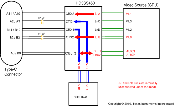 Figure 9. SOURCE Pin Assignment Option D and F (AMSEL = L, EN = H, POL = L)
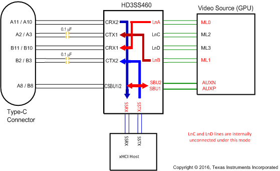 Figure 10. SOURCE Pin Assignment Option D and F (AMSEL = L, EN = H, POL = H)
Table 4. SINK Pin Assignment Option C (AMSEL = H, EN = H)
| RECEPTACLE PIN NUMBER | 460 PIN MAPPING TO TYPE C CONNECTOR | 460 PIN MAPPING TO DP SOURCE (GPU) | |
|---|---|---|---|
| POL = L | POL = H | ||
| A11/10 | CRX2 | LnA(ML1) | LnD(ML2) |
| A2/3 | CTX1 | LnC(ML3) | LnB(ML0) |
| B11/10 | CRX1 | LnD(ML2) | LnA(ML1) |
| B2/3 | CTX2 | LnB(ML0) | LnC(ML3) |
| A8 | CSBU1 | SBU1(AUXN) | SBU2(AUXP) |
| B8 | CSBU2 | SBU2(AUXP) | SBU1(AUXN) |
 Figure 11. SINK Pin Assignment Option C (AMSEL = H, EN = H)
Table 5. SINK Pin Assignment Option D (AMSEL = L, EN = H)
| RECEPTACLE PIN NUMBER | 460 PIN MAPPING TO TYPE C CONNECTOR | 460 PIN MAPPING TO DP SOURCE (GPU) | |
|---|---|---|---|
| POL = L | POL = H | ||
| A11/10 | CRX2 | LnA(ML1) | SSRX |
| A2/3 | CTX1 | SSTX | LnB(ML0) |
| B11/10 | CRX1 | SSRX | LnA(ML1) |
| B2/3 | CTX2 | LnB(ML0) | SSTX |
| A8 | CSBU1 | SBU1(AUXN) | SBU2(AUXP) |
| B8 | CSBU2 | SBU2(AUXP) | SBU1(AUXN) |
Space
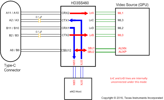 Figure 12. SINK Pin Assignment Option D
 (AMSEL = L, EN = H, POL=L)
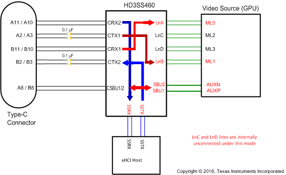 Figure 13. SINK Pin Assignment Option D
(AMSEL = L, EN = H, POL=H)
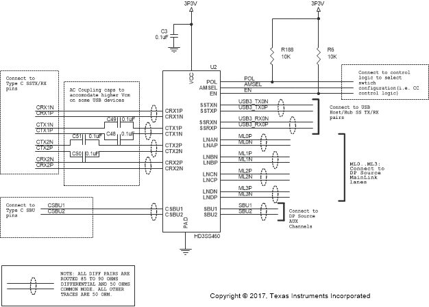
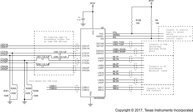
Schematic diagrams Figure 14, Figure 15, and Figure 16 show the DP Source/USB Host implementation; and, Figure 17, Figure 18, and Figure 19 show the DP Sink/USB Device/HUSB Hub/Dock implementation, respectively.
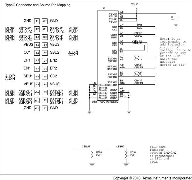 Figure 14. Schematic Implementations for DP Source/ USB Host (1 of 3)
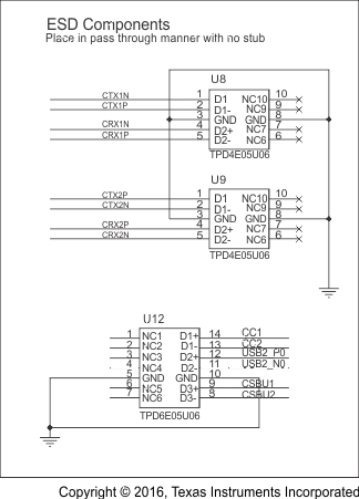 Figure 15. Schematic Implementations for DP Source/ USB Host (2 of 3)
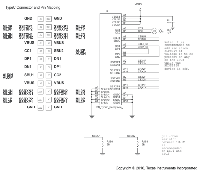 Figure 17. Schematic Implementations for DP Sink/ USB Device/HUB/Dock (1 of 3)
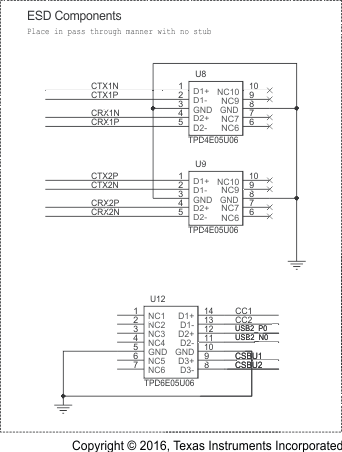 Figure 18. Schematic Implementations for DP Sink/ USB Device/HUB/Dock (2 of 3)
