ZHCSDI9D January 2015 – January 2017 HD3SS460
PRODUCTION DATA.
11 Layout
11.1 Layout Guidelines
High performance layout practices are paramount for board layout for high speed signals to ensure good signal integrity. Even minor imperfection can cause impedance mismatch resulting reflection. Special care is warranted for traces, connections to device, and connectors.
11.1.1 Critical Routing
The high speed differential signals must be routed with great care to minimize signal quality degradation between the connector and the source or sink of the high speed signals by following the guidelines provided in this document. Depending on the configuration schemes, the speed of each differential pair can reach a maximum speed of 5.4 Gbps. These signals are to be routed first before other signals with highest priority.
- Each differential pair should be routed together with controlled differential impedance of 85 to 90-Ω and 50-Ω common mode impedance. Keep away from other high speed signals. The number of vias should be kept to minimum. Each pair should be separated from adjacent pairs by at least 3 times the signal trace width. Route all differential pairs on the same group of layers (Outer layers or inner layers) if not on the same layer. No 90 degree turns on any of the differential pairs. If bends are used on high speed differential pairs, the angle of the bend should be greater than 135 degrees.
- Length matching:
- Keep high speed differential pairs lengths within 5 mil of each other to keep the intra-pair skew minimum.
- The inter-pair matching of the differential pairs is not as critical as intra-pair matching. The SSTX and SSRX pairs do not have to match while they need to be routed as short as possible.
- Keep high speed differential pair traces adjacent to ground plane.
- Do not route differential pairs over any plane split
- ESD components on the high speed differential lanes should be placed nearest to the connector in a pass through manner without stubs on the differential path. In order to control impedance for transmission lines, a solid ground plane should be placed next to the high- speed signal layer. This also provides an excellent low-inductance path for the return current flow.
- Placement recommendation would be: Connector – ESD Components --- HD3SS460
- For ease of routing, the P and N connection of the USB3.1 differential pairs to the HD3SS460 pins can be swapped as long as the corresponding pairs are swapped on the other end of the switch The example is shown in the reference EVM schematics section of this document. The P/N can be swapped on USB 3.1 connection of the switch for ease of routing purposes.
11.1.2 General Routing/Placement Rules
- Route all high-speed signals first on un-routed PCB: SSTXP/N, SSRXT/N, LNAP/N, LNB P/N, LNC P/N, LND P/N, CTX*P/N. The stub on USB2 D+ and D- pairs should not exceed 3.5mm.
- Follow 20H rule (H is the distance to reference plane) for separation of the high-speed trace from the edge of the plane
- Minimize parallelism of high speed clocks and other periodic signal traces to high speed lines
- All differential pairs should be routed on the top or bottom layer (microstrip traces) if possible or on the same group of layers. Vias should only be used in the breakout region of the device to route from the top to bottom layer when necessary. Avoid using vias in the main region of the board at all cost. Use a ground reference via next to signal via. Distance between ground reference via and signal need to be calculated to have similar impedance as traces.
- All differential signals should not be routed over plane split. Changing signal layers is preferable to crossing plane splits.
- Use of and proper placement of stitching caps when split plane crossing is unavoidable to account for high-frequency return current path
- Route differential traces over a continuous plane with no interruptions.
- Do not route differential traces under power connectors or other interface connectors, crystals, oscillators, or any magnetic source.
- Route traces away from etching areas like pads, vias, and other signal traces. Try to maintain a 20 mil keep- out distance where possible.
- Decoupling capacitors should be placed next to each power terminal on the HD3SS460. Care should be taken to minimize the stub length of the trace connecting the capacitor to the power pin.
- Avoid sharing vias between multiple decoupling capacitors.
- Place vias as close as possible to the decoupling capacitor solder pad.
- Widen VCC/GND planes to reduce effect of static and dynamic IR drop.
- The VBUS traces/planes must be wide enough to carry maximum of 2 A current.
11.2 Layout Example
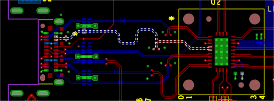
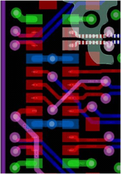
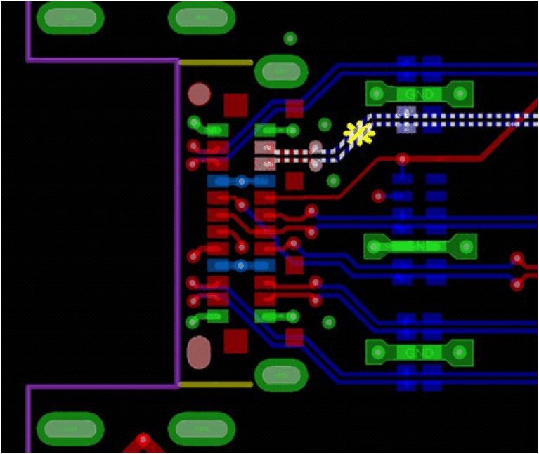
Figure 20, Figure 21, and Figure 22 illustrate some guidelines for layout. Actual layout should be optimized for various factors such as board geometry, connector type, and application.
 Figure 20. USB Type C Connector to HD3SS460 Signal Routing
 Figure 21. Dual SMT Mid-Mount Type C Connector Layout Example Zoom-in
 Figure 22. Dual-row SMT Mid-mount Type C with ESD Components