ZHCSDI9D January 2015 – January 2017 HD3SS460
PRODUCTION DATA.
8 Detailed Description
8.1 Overview
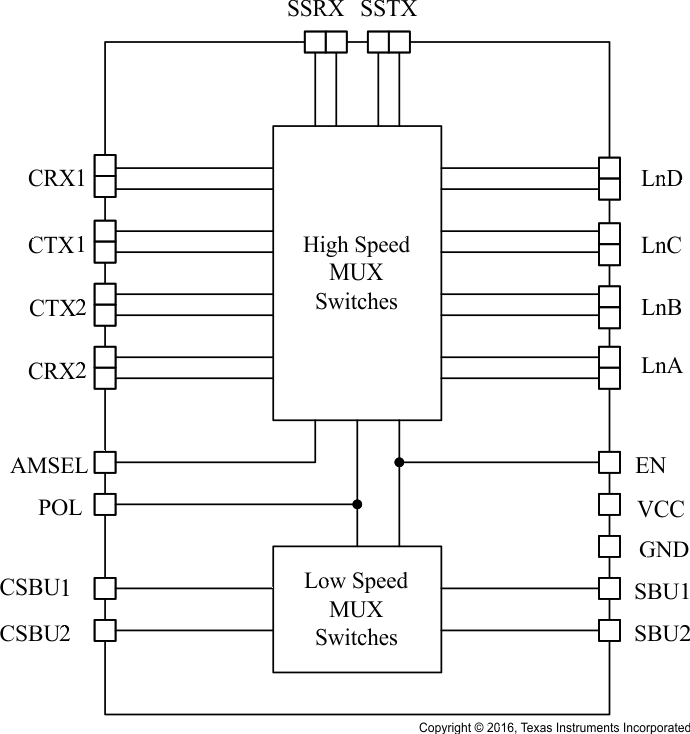
The HD3SS460 is a high-speed bi-directional passive 4-6 cross-point switch in mux or demux configurations. Based on control pin POL the device provides switching to accommodate USB Type-C plug flipping. The device provides multiple signal switching options that allow system implementation flexibility.
The HD3SS460 is a generic analog, differential passive switch that can work for any high speed interface applications as long as it is biased at a common mode voltage range of 0-2 V and has differential signaling with differential amplitude up to 1800 mVpp. It employs an adaptive tracking that ensures the channel remains unchanged for entire common mode voltage range
Excellent dynamic characteristics of the device allow high speed switching with minimum attenuation to the signal eye diagram with very little added jitter.
8.2 Functional Block Diagram
8.3 Feature Description
8.3.1 High Speed Differential Signal Switching
Based on control pin AMSEL the device provides muxing options of:
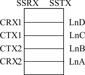
- 1 port (RX and TX) USB3.1 SS data / 2Ch video (or any other Alternate Mode data)
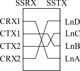
- All 4Ch video (or any other Alternate Mode data)
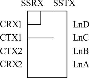
- 1 port (RX and TX) USB3.1 SS data
- 1 port (RX and TX) USB3.1 SS data / 2Ch video (or any other Alternate Mode data) with option of choosing video from two different source/sink
- 1 port (RX and TX) USB3.1 SS data / 2Ch video (or any other Alternate Mode data) with option of choosing video 2 Ln Video or 1 Ln Video from two different source/sink
8.3.2 Low Speed SBU Signal Switching
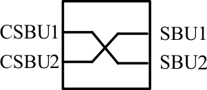
The device also provides cross point muxing for low speed SBU signals as needed in USB Type-C flippable connector implementation. The device provides the option to choose the USB only implementation where SBU ports are in tri-state.
8.3.3 Output Enable and Power Savings
The HD3SS460 has two power modes, active/normal operating mode and standby/shutdown mode. During standby mode, the device consumes very little current to save the maximum power. To enter standby mode, the EN control pin is pulled low and must remain low. For active/normal operation, the EN control pin should be pulled high to VDD through a resistor or dynamically controlled to switch between H or M.
HD3SS460 consumes <2 mW of power when operational and <5 µW in shutdown mode, exercisable by the EN pin.
8.4 Device Functional Modes
8.4.1 Device High Speed Switch Control Modes
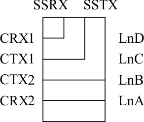
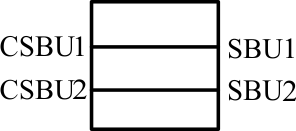
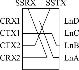
Table 1. MUX Control for High Speed and Low Speed SBU Channels
| POL | AMSEL | EN | CONFIGURATIONS | HIGH SPEED SIGNAL FLOW(1) | SBU SIGNAL FLOW |
|---|---|---|---|---|---|
| L | L | H | 2CH USBSS + 2CH AM (Normal) |
 |
 |
| H | L | H | 2CH USBSS + 2CH AM (Flipped) |
 |
 |
| L | H | H | 4CH AM (Normal) |
 |
 |
| H | H | H | 4CH AM (Flipped) |
 |
 |
| L | M | H | 2CH USBSS (Normal) |
 |
All Low Speed SBU Ports HighZ |
| H | M | H | 2CH USBSS (Flipped) |
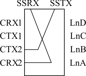 |
All Low Speed SBU Ports HighZ |
| L | M | M | 2CH USBSS + 2CH AM (Normal) |
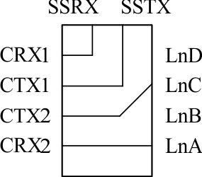 |
 |
| H | M | M | 2CH USBSS + 2CH AM (Flipped) |
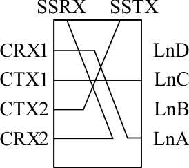 |
 |
| L | L | M | 2CH USBSS + 2CH AM from alternate GPU (Normal) |
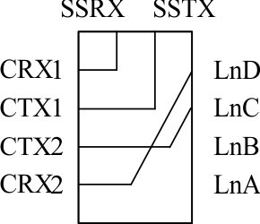 |
 |
| H | L | M | 2CH USBSS + 2CH AM from alternate GPU (Flipped) |
 |
 |
| L | H | M | Reserved | Reserved | Reserved |
| H | H | M | Reserved | Reserved | Reserved |
| X | X | L | All High Speed Ports HighZ | All High Speed Ports HighZ | All Low Speed SBU Ports HighZ |