ZHCSDJ6E February   2015  – June 2018 LMH1218

PRODUCTION DATA.  

  1. 特性
  2. 应用
  3. 说明
    1.     Device Images
      1.      简化 SPI 电路原理图
  4. 修订历史记录
  5. Pin Configuration and Functions
    1.     Pin Descriptions – SPI Mode/ Mode_SEL = 1 kΩ to VDD
    2.     Pin Descriptions – SMBUS Mode/ MODE_SEL = 1 kΩ to GND
  6. Specifications
    1. 6.1 Absolute Maximum Ratings
    2. 6.2 ESD Ratings
    3. 6.3 Recommended Operating Conditions
    4. 6.4 Thermal Information
    5. 6.5 Electrical Characteristics
    6. 6.6 Recommended SMBus Interface AC Timing Specifications
    7. 6.7 Serial Parallel Interface (SPI) Bus Interface AC Timing Specifications
    8. 6.8 Typical Characteristics
  7. Detailed Description
    1. 7.1 Overview
    2. 7.2 Functional Block Diagram
    3. 7.3 Feature Description
      1. 7.3.1 Loss of Signal Detector
      2. 7.3.2 Continuous Time Linear Equalizer (CTLE)
      3. 7.3.3 2:1 Multiplexer
      4. 7.3.4 Clock and Data Recovery
      5. 7.3.5 Eye Opening Monitor (EOM)
      6. 7.3.6 Fast EOM
        1. 7.3.6.1 SMBus Fast EOM Operation
        2. 7.3.6.2 SPI Fast EOM Operation
      7. 7.3.7 LMH1218 Device Configuration
        1. 7.3.7.1 MODE_SEL
        2. 7.3.7.2 ENABLE
        3. 7.3.7.3 LOS_INT_N
        4. 7.3.7.4 LOCK
        5. 7.3.7.5 SMBus MODE
        6. 7.3.7.6 SMBus READ/WRITE Transaction
        7. 7.3.7.7 SPI Mode
          1. 7.3.7.7.1 SPI READ/WRITE Transaction
          2. 7.3.7.7.2 SPI Write Transaction Format
          3. 7.3.7.7.3 SPI Read Transaction Format
        8. 7.3.7.8 SPI Daisy Chain
          1. 7.3.7.8.1 SPI Daisy Chain Write Example
          2. 7.3.7.8.2 SPI Daisy Chain Write Read Example
            1. 7.3.7.8.2.1 SPI Daisy Chain Length of Daisy Chain Illustration
      8. 7.3.8 Power-On Reset
    4. 7.4 Device Functional Modes
    5. 7.5 Programming
    6. 7.6 Register Maps
      1. 7.6.1 Global Registers
      2. 7.6.2 Receiver Registers
      3. 7.6.3 CDR Registers
      4. 7.6.4 Transmitter Registers
  8. Application and Implementation
    1. 8.1 Application Information
      1. 8.1.1 General Guidance for All Applications
    2. 8.2 Typical Application
      1. 8.2.1 Design Requirements
      2. 8.2.2 Detailed Design Procedure
      3. 8.2.3 Application Curves
    3. 8.3 Do's and Don'ts
    4. 8.4 Initialization Set Up
      1. 8.4.1 Selective Data Rate Lock
  9. Power Supply Recommendations
  10. 10Layout
    1. 10.1 Layout Guidelines
    2. 10.2 Layout Example
    3. 10.3 Solder Profile
  11. 11器件和文档支持
    1. 11.1 器件支持
      1. 11.1.1 开发支持
    2. 11.2 文档支持
      1. 11.2.1 相关文档
    3. 11.3 接收文档更新通知
    4. 11.4 社区资源
    5. 11.5 商标
    6. 11.6 静电放电警告
    7. 11.7 术语表
  12. 12机械、封装和可订购信息

SPI Daisy Chain

The LMH1218 includes an enhanced SPI controller that supports daisy-chaining the serial configuration data among multiple LMH1218 devices. The LMH1218 device supports SPI Daisy Chain between devices with an 8-bit SPI addressing scheme. Each LMH1218 device is directly connected to the SCK and SS_N pins of the Host. However, only the first LMH1218 device in the chain is connected to the Host’s MOSI pin, and only the last device in the chain is connected to the Host’s MISO pin. The MOSI pin of each intermediate LMH1218 device in the chain is connected to the MISO pin of the previous LMH1218 device, thereby creating a serial shift register. This architecture is shown in Figure 18:
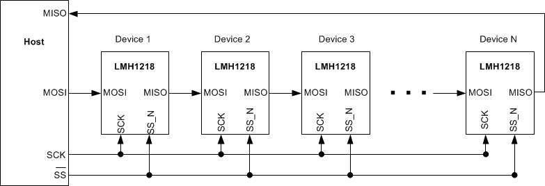
LMH1218 daisy_chain_updated_020415.gifFigure 18. Daisy-Chain Configuration

In a daisy-chain configuration of N LMH1218 devices, the Host conceptually sees a long shift register of length 17xN. Therefore the length of a Basic SPI Transaction, as described above, is 17xN; in other words, SS_N is asserted for 17xN clock cycles.