ZHCSDJ6E February   2015  – June 2018 LMH1218

PRODUCTION DATA.  

  1. 特性
  2. 应用
  3. 说明
    1.     Device Images
      1.      简化 SPI 电路原理图
  4. 修订历史记录
  5. Pin Configuration and Functions
    1.     Pin Descriptions – SPI Mode/ Mode_SEL = 1 kΩ to VDD
    2.     Pin Descriptions – SMBUS Mode/ MODE_SEL = 1 kΩ to GND
  6. Specifications
    1. 6.1 Absolute Maximum Ratings
    2. 6.2 ESD Ratings
    3. 6.3 Recommended Operating Conditions
    4. 6.4 Thermal Information
    5. 6.5 Electrical Characteristics
    6. 6.6 Recommended SMBus Interface AC Timing Specifications
    7. 6.7 Serial Parallel Interface (SPI) Bus Interface AC Timing Specifications
    8. 6.8 Typical Characteristics
  7. Detailed Description
    1. 7.1 Overview
    2. 7.2 Functional Block Diagram
    3. 7.3 Feature Description
      1. 7.3.1 Loss of Signal Detector
      2. 7.3.2 Continuous Time Linear Equalizer (CTLE)
      3. 7.3.3 2:1 Multiplexer
      4. 7.3.4 Clock and Data Recovery
      5. 7.3.5 Eye Opening Monitor (EOM)
      6. 7.3.6 Fast EOM
        1. 7.3.6.1 SMBus Fast EOM Operation
        2. 7.3.6.2 SPI Fast EOM Operation
      7. 7.3.7 LMH1218 Device Configuration
        1. 7.3.7.1 MODE_SEL
        2. 7.3.7.2 ENABLE
        3. 7.3.7.3 LOS_INT_N
        4. 7.3.7.4 LOCK
        5. 7.3.7.5 SMBus MODE
        6. 7.3.7.6 SMBus READ/WRITE Transaction
        7. 7.3.7.7 SPI Mode
          1. 7.3.7.7.1 SPI READ/WRITE Transaction
          2. 7.3.7.7.2 SPI Write Transaction Format
          3. 7.3.7.7.3 SPI Read Transaction Format
        8. 7.3.7.8 SPI Daisy Chain
          1. 7.3.7.8.1 SPI Daisy Chain Write Example
          2. 7.3.7.8.2 SPI Daisy Chain Write Read Example
            1. 7.3.7.8.2.1 SPI Daisy Chain Length of Daisy Chain Illustration
      8. 7.3.8 Power-On Reset
    4. 7.4 Device Functional Modes
    5. 7.5 Programming
    6. 7.6 Register Maps
      1. 7.6.1 Global Registers
      2. 7.6.2 Receiver Registers
      3. 7.6.3 CDR Registers
      4. 7.6.4 Transmitter Registers
  8. Application and Implementation
    1. 8.1 Application Information
      1. 8.1.1 General Guidance for All Applications
    2. 8.2 Typical Application
      1. 8.2.1 Design Requirements
      2. 8.2.2 Detailed Design Procedure
      3. 8.2.3 Application Curves
    3. 8.3 Do's and Don'ts
    4. 8.4 Initialization Set Up
      1. 8.4.1 Selective Data Rate Lock
  9. Power Supply Recommendations
  10. 10Layout
    1. 10.1 Layout Guidelines
    2. 10.2 Layout Example
    3. 10.3 Solder Profile
  11. 11器件和文档支持
    1. 11.1 器件支持
      1. 11.1.1 开发支持
    2. 11.2 文档支持
      1. 11.2.1 相关文档
    3. 11.3 接收文档更新通知
    4. 11.4 社区资源
    5. 11.5 商标
    6. 11.6 静电放电警告
    7. 11.7 术语表
  12. 12机械、封装和可订购信息

Layout Example

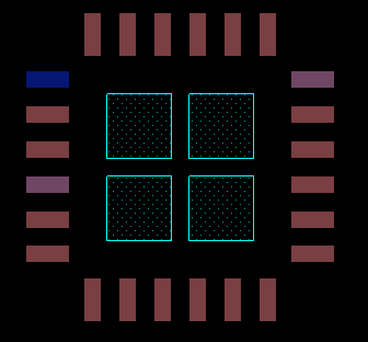
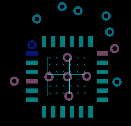
The following example layout demonstrates how the thermal pad should be laid out using standard WQFN board routing guidelines.
LMH1218 layout_example_1.png
Note: Thermal pad is divided into 4 squares with solder paste
Figure 28. LMH1218 Recommended Four Squares Solder Paste
LMH1218 layout_example2.png
5 Vias without solder paste are located between 4 squares solder paste
Figure 29. LMH1218 Recommended Solder Paste Mask and Vias
LMH1218 example_layout.png
Top etch plus traces
Figure 30. Example Layout