ZHCSDL7B November 2014 – March 2016 AMC7834
PRODUCTION DATA.
- 1 特性
- 2 应用范围
- 3 说明
- 4 修订历史记录
- 5 Pin Configuration and Functions
-
6 Specifications
- 6.1 Absolute Maximum Ratings
- 6.2 ESD Ratings
- 6.3 Recommended Operating Conditions
- 6.4 Thermal Information
- 6.5 Electrical Characteristics—DAC Specifications
- 6.6 Electrical Characteristics—ADC, Current and Temperature Sensor Specifications
- 6.7 Electrical Characteristics—General Specifications
- 6.8 Serial Interface Timing Requirements
- 6.9 Switching Characteristics—DAC Specifications
- 6.10 Switching Characteristics—ADC, Current and Temperature Sensor Specifications
- 6.11 Switching Characteristics—General Specifications
- 6.12 Typical Characteristics
-
7 Detailed Description
- 7.1 Overview
- 7.2 Functional Block Diagram
- 7.3 Feature Description
- 7.4 Device Functional Modes
- 7.5 Programming
- 7.6
Register Maps
- 7.6.1 Power Mode: Address 0x02
- 7.6.2 Device Identification: Address 0x04 through 0x0C
- 7.6.3
General Device Configuration: Address 0x10 through 0x16
- 7.6.3.1 AMC Configuration 0 Register (address = 0x10) [reset = 0x0300]
- 7.6.3.2 AMC Configuration 1 Register (address = 0x11) [reset = 0x036A]
- 7.6.3.3 ADC MUX Register (address = 0x12) [reset = 0x0000]
- 7.6.3.4 Closed Loop Settling Time Register (address = 0x14) [reset = 0x2222]
- 7.6.3.5 DAC Sync Register (address = 0x15) [reset = 0x0000]
- 7.6.3.6 DAC Range Register (address = 0x16) [reset = 0x0000]
- 7.6.4
Clamp and Alarm Configuration: Address 0x17 through 0x1B
- 7.6.4.1 CLAMP Configuration Register (address = 0x17) [reset = 0x003F]
- 7.6.4.2 SLEEP1 Configuration Register (address = 0x18) [reset = 0xFF00]
- 7.6.4.3 SLEEP2 Configuration Register (address = 0x19) [reset = 0xFF00]
- 7.6.4.4 ALARMOUT Clamp Register (address = 0x1A) [reset = 0x0000]
- 7.6.4.5 ALARMOUT Configuration Register (address = 0x1B) [reset = 0x0000]
- 7.6.5 Conversion Trigger: Address 0x1C
- 7.6.6 Reset: Address 0x1D
- 7.6.7 Device Status: Address 0x1E and 0x1F
- 7.6.8
ADC Data: Address 0x20 through 0x2F
- 7.6.8.1 ADCn-Internal-Data Register (address = 0x20 to 0x23) [reset = 0x0000]
- 7.6.8.2 ADCn-External-Data Register (address = 0x24 to 0x27) [reset = 0x0000]
- 7.6.8.3 CSn-Data Register (address = 0x28 to 0x2B) [reset = 0x0000]
- 7.6.8.4 LT-Data Register (address = 0x2D) [reset = 0x0000]
- 7.6.8.5 RTn-Data Register (address = 0x2E to 0x2F) [reset = 0x0000]
- 7.6.9 DAC Data: Address 0x30 through 0x37
- 7.6.10 Closed-Loop Control: Address 0x38 through 0x3B
- 7.6.11
Alarm Threshold Configuration: Address 0x40 through 0x4F
- 7.6.11.1 ADCINTn/CSn-Upper-Threshold Register (address = 0x40, 0x42, 0x44 and 0x46) [reset = 0x0FFF]
- 7.6.11.2 ADCINTn/CSn-Lower-Threshold Register (address = 0x41, 0x43, 0x45 and 0x47) [reset = 0x0000]
- 7.6.11.3 TS-Upper-Threshold Register (address = 0x48, 0x4A and 0x4C) [reset = 0x07FF]
- 7.6.11.4 TS-Lower-Threshold Register (address = 0x49, 0x4B and 0x4D) [reset = 0x0800]
- 7.6.11.5 DACnn-Upper-Threshold Register (address = 0x4E and 0x4F) [reset = 0x0FFF]
- 7.6.12 Alarm Hysteresis Configuration: Address 0x50 and 0x56
- 7.6.13 GPIO: Address 0x58
- 8 Application and Implementation
- 9 Power Supply Recommendations
- 10Layout
- 11器件和文档支持
- 12机械、封装和可订购信息
8 Application and Implementation
NOTE
Information in the following applications sections is not part of the TI component specification, and TI does not warrant its accuracy or completeness. TI’s customers are responsible for determining suitability of components for their purposes. Customers should validate and test their design implementation to confirm system functionality.
8.1 Application Information
The AMC7834 device is a highly integrated, low-power, analog monitoring and control solution that includes one multi-channel 12-bit ADC, eight 12-bit DACs, four high-side current-sense amplifiers and temperature sensing capabilities. The AMC7834 typical application is power amplifier biasing in wireless base stations, however its high level integration make it a good solution for many different systems ranging from industrial control sytems to test-and-measurement units.
The power amplifiers (PAs) used in wireless infrastructure include transistor technologies that are extremely temperature sensitive, and require DC biasing circuits to optimize RF performance, power efficiency, and stability. The AMC7834 device provides eight DAC channels that can be used to bias the inputs of the power amplifiers. The device also includes two remote temperature sensing interfaces, one internal local temperature sensor, four high-side current-sensing channels, and four ADC channels for general-purpose monitoring.
Current sensing and temperature sensing are the two main monitoring schemes for PA bias compensation. The PA drain current is monitored by measuring the differential voltage drop accross a shunt resistor. The AMC7834 internal local-temperature sensor and two remote-sensor driver inputs can be used to detect temperature variations during PA operation. Figure 103 shows the circuit diagram of this system.
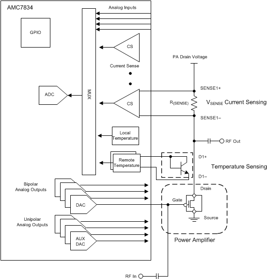 Figure 103. AMC7834 Example PA Bias System
8.2 Typical Application
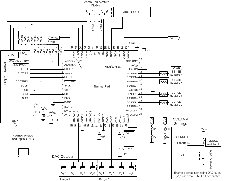 Figure 104. AMC7834 Example Schematic
8.2.1 Design Requirements
The AMC7834 example schematic uses the majority of the design parameters listed in Table 50.
Table 50. Design Parameters
| DESIGN PARAMETER | EXAMPLE VALUE |
|---|---|
| AVCC | 5 V |
| IOVDD | 3.3 V |
| DVDD | 5 V |
| AVDD | 5 V |
| AVSS | –5 V |
| 4 External unipolar inputs | ADC[1-4]: 0 to 2.5 V range |
| 4 High-Side Current Sense | Differential input of 0 to 200 mV |
| 4 bipolar DAC outputs | –4 to 1 V, –5 to 0 V, and 0 to 5 V |
| 4 unipolar DAC outputs | 0 to 5 V, 2.5 to 7.5 V |
| Remote temperature sensing | Two remote temperature diode drivers |
8.2.2 Detailed Design Procedure
Use the following parameters to facilitate the design process:
- AVCC and AVSS voltage values
- ADC and high-side current-sense input voltage range
- DAC output voltage ranges
- Remote temperature applications
8.2.2.1 ADC Input Conditioning
The AMC7834 monitoring system is centered on a single ADC core that features a multichannel input stage to a successive approximation register (SAR) ADC. The analog inputs include four external analog inputs, four internal inputs for bipolar DAC monitoring, four high-side current-sense amplifiers for PA current monitoring, two remote temperature sensors, and an internal analog temperature sensor.
The external analog inputs (ADC1 through ADC4) feature a range of 0 to Vref (Vref corresponds to either an external 2.5 V reference or the device internal reference), while the internal inputs accept a full-scale range of –5 to 2.5 V. The current-sense inputs feature a 4 to 60 V common-mode voltage range, and accept a differential input range of 0 to 200 mV. A 4.7 µF capacitor is recommended between the REF_CMP pin and the AGND4 pin. The value of this capacitor must exceed 470 nF to ensure reference stability. A high-quality ceramic capacitor, type NP0 or X7R, is recommended because of the optimal performance of the capacitor across temperature and very-low dissipation factor.
It is recommended that all external analog inputs are driven with a low impedance source to ensure correct functionality. In applications where the signal-source impedance is high, the analog inputs can be conditioned through a buffer amplifier, such as a voltage follower.
8.2.2.2 DAC Output Range Selection
The AMC7834 device has four bipolar and four unipolar DACs with programmable output ranges. The bipolar DACs feature the ranges –4 to 1 V, –5 to 0 V, and 0 to 5 V. The unipolar DACs feature the ranges 0 to 5 V and 2.5 to 7.5 V. The DAC ranges are configurable by setting the DAC range register (see the DAC Range Register (address = 0x16) [reset = 0x0000] section).
The maximum source and sink capability of the DAC internal amplifiers are listed as part of the DAC output characteristics in the Electrical Characteristics—DAC Specifications table.
The graph in the Application Performance Curve section show the relationship of both stability and settling time with different capacitive and resistive loading structures.
8.2.2.3 Temperature Sensing Applications
The AMC7834 has one local temperature and two temperature diode drivers, as well as four external analog inputs that are easily configurable to remote temperature sensor circuits. The integrated temperature sensor, remote temperature sensor, and analog input registers automatically update with every conversion. Figure 105 shows a typical setup for the two temperature diode-driver inputs. Additional noise filtering can be achieved by placing a bypass capacitor across the inputs of the remote temperature sensors. A high-quality ceramic capacitor, type NP0 or X7R, is recommended because of the optimal performance of the capacitor across temperature. See the Remote Temperature Sensors section for a details.
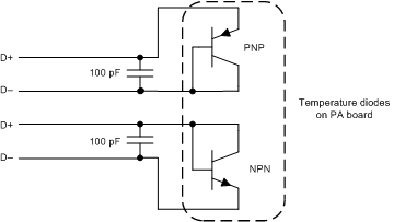 Figure 105. Remote Temperature Sensors (PNP and NPN)
Additionally, the ADC inputs can be used to accept voltage from other temperature-sensing IC circuits as shown in Figure 106. The temperature sensor use for analog input conditioning in this example is the LM50 device which is a high precision integrated-circuit temperature sensor that can sense a –40°C to +125°C temperature range using a single positive supply. The full-scale output of the temperature sensor ranges from 100 mV to 1.75 V for a –40°C to +125°C temperature range. In an extremely noisy environment, adding some filtering to minimize noise pickup may be necessary. A typical recommended value for the bypass capacitor is 0.1 µF from the V+ pin to ground. A high-quality ceramic capacitor, type NP0 or X7R, is recommended because of the optimal performance of the capacitor across temperature and very-low dissipation factor.
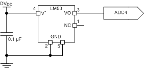 Figure 106. Temperature Sense Application With LM50
8.2.2.4 Current Sensing Applications
The AMC7834 device also features four high-side current-sense amplifiers that support common-mode voltages from 4 to 60 V and a full-scale sense voltage of 0 to 200 mV. In applications that require current sensing across a power amplifier, the SENSE± differential inputs connect across a resistor to sense small differential voltage that is proportional to current across the PA as shown in Figure 107. The current-sense conversion results are stored in the Current sense data registers. The current sensors are also configurable as closed-loop drain current controllers. See the Current Sensors section for details.
Figure 107 shows a method of separating the drain voltage from the power amplifier with a series PMOS transistor. The activation of the PMOS connects the PAVDD voltage supply to the drain pin of the power amplifier. The PMOS is driven with a voltage divider that swings from PAVDD to PAVDD(R2 / [R1 + R2]). The NMOS shown in Figure 107 is connected to the PA_ON output which controls the state of the PMOS transistor.
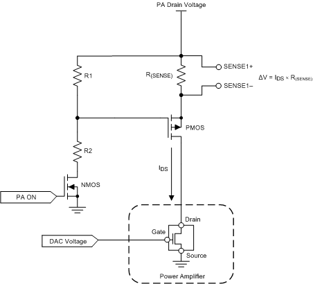 Figure 107. Current Sense (SENSE) Connections With PMOS ON and OFF
8.2.3 Application Performance Curve
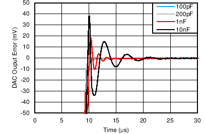
| Code 0x000 to 0xFFF to within 0.5% of final value |
8.3 Initialization Set Up
8.3.1 Initialization Procedure
- Supply all voltages (PAVDD, AVDD, DVDD, IOVDD, AVCC, AVSS) and clamp inputs (VCLAMP1 and VCLAMP2). The AMC7834 does not require a specific supply sequencing.
- A 250 µs POR delay occurs after a minimum AVDD supply of 4.5 V has been applied. Do not attempt serial communication during this time.
- It is recommended to issue a hardware or software-reset.
- Wait for completion of the reset operation (at least 250 µs for a hardware reset or at least 10 µs for a software reset).
- After reset, the following conditions are met:
- The device is in open-loop mode and all DAC data registers are set to all zeros.
- All DAC outputs are set to the clamp value regardless of the SLEEP1 and SLEEP2 pin levels.
- The PA_ON signal is set to the OFF state.
- If not already done so, it is recommended to tie the SLEEP1 and SLEEP2 pins low.
- Configure the AMC7834 without the DACs leaving clamp mode.
- If the PA_ON control signal is enabled, switch the PA_ON signal to the ON state. By default, the AVSS supply must be present to enable the PA_ON signal to enter the ON state.
- Release the DACs out of clamp mode.
- Verify that the ADC has entered the READY state.
- Issue an ADC trigger signal to initiate conversion of the monitoring inputs.
After initialization the AMC7834 allows switching between open-loop and closed-loop operation. However, before switching between operating modes, it is strongly recommended to clamp the bipolar DAC outputs, stop the ADC conversion cycle, and if applicable, switch the PA_ON signal to the OFF state. To resume operation follow steps 7 through 11 of the Initialization Procedure.