ZHCSDM2A November   2014  – December 2014 TPS63024 , TPS630241 , TPS630242

PRODUCTION DATA.  

  1. 特性
  2. 应用范围
  3. 说明
  4. 修订历史记录
  5. Pin Configuration and Functions
  6. Specifications
    1. 6.1 Absolute Maximum Ratings
    2. 6.2 ESD Ratings
    3. 6.3 Recommended Operating Conditions
    4. 6.4 Thermal Information
    5. 6.5 Electrical Characteristics
    6. 6.6 Timing Requirements
    7. 6.7 Typical Characteristics
  7. Detailed Description
    1. 7.1 Overview
    2. 7.2 Functional Block Diagram
    3. 7.3 Feature Description
      1. 7.3.1 Undervoltage Lockout (UVLO)
      2. 7.3.2 Output Discharge Function
      3. 7.3.3 Thermal Shutdown
      4. 7.3.4 Softstart
      5. 7.3.5 Short Circuit Protection
    4. 7.4 Device Functional Modes
      1. 7.4.1 Control Loop Description
      2. 7.4.2 Power Save Mode Operation
      3. 7.4.3 Current Limit
      4. 7.4.4 Supply and Ground
      5. 7.4.5 Device Enable
  8. Application and Implementation
    1. 8.1 Application Information
    2. 8.2 Typical Application
      1. 8.2.1 Design Requirements
      2. 8.2.2 Detailed Design Procedure
        1. 8.2.2.1 Output Filter Design
        2. 8.2.2.2 Inductor Selection
        3. 8.2.2.3 Capacitor Selection
          1. 8.2.2.3.1 Input Capacitor
          2. 8.2.2.3.2 Output Capacitor
        4. 8.2.2.4 Setting The Output Voltage
      3. 8.2.3 Application Curves
  9. Power Supply Recommendations
  10. 10Layout
    1. 10.1 Layout Guidelines
    2. 10.2 Layout Example
  11. 11器件和文档支持
    1. 11.1 器件支持
      1. 11.1.1 Third-Party Products Disclaimer
    2. 11.2 文档支持
      1. 11.2.1 相关文档 
    3. 11.3 相关链接
    4. 11.4 商标
    5. 11.5 静电放电警告
    6. 11.6 Glossary
  12. 12机械、封装和可订购信息

Pin Configuration and Functions

WCSP
20-Pin
YFF (TOP VIEW)
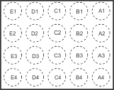
TPS63024 TPS630241 TPS630242 TPS63025pinout2.gif

Pin Functions

PIN I/O DESCRIPTION
NAME NO.
VOUT A1,A2,A3 PWR Buck-boost converter output
FB A4 IN Voltage feedback of adjustable version, must be connected to VOUT for fixed output voltage versions
L2 B1,B2,B3 PWR Connection for Inductor
PFM/PWM B4 IN set low for PFM mode, set high for forced PWM mode. It must not be left floating
PGND C1,C2,C3 PWR Power Ground
GND C4 PWR Analog Ground
L1 D1,D2,D3 PWR Connection for Inductor
EN D4 IN Enable input. Set high to enable and low to disable. It must not be left floating.
VIN E1,E2,E3 PWR Supply voltage for power stage
VINA E4 PWR Supply voltage for control stage.