ZHCSDO1 May   2015 LM2775

PRODUCTION DATA.  

  1. 特性
  2. 应用
  3. 说明
  4. 修订历史记录
  5. Pin Configuration and Functions
  6. Specifications
    1. 6.1 Absolute Maximum Ratings
    2. 6.2 ESD Ratings
    3. 6.3 Recommended Operating Conditions
    4. 6.4 Thermal Information
    5. 6.5 Electrical Characteristics
    6. 6.6 Switching Characteristics
    7. 6.7 Typical Characteristics
  7. Detailed Description
    1. 7.1 Overview
    2. 7.2 Functional Block Diagram
    3. 7.3 Feature Description
      1. 7.3.1 Pre-Regulation
      2. 7.3.2 Input Current Limit
      3. 7.3.3 PFM Mode
      4. 7.3.4 Output Discharge
      5. 7.3.5 Thermal Shutdown
      6. 7.3.6 Undervoltage Lockout
    4. 7.4 Device Functional Modes
      1. 7.4.1 Shutdown
      2. 7.4.2 Boost Mode
  8. Application and Implementation
    1. 8.1 Application Information
    2. 8.2 Typical Application
      1. 8.2.1 Design Requirements
      2. 8.2.2 Detailed Design Procedure
        1. 8.2.2.1 Output Current Capability
        2. 8.2.2.2 Efficiency
        3. 8.2.2.3 Power Dissipation
        4. 8.2.2.4 Recommended Capacitor Types
        5. 8.2.2.5 Output Capacitor and Output Voltage Ripple
        6. 8.2.2.6 Input Capacitor and Input Voltage Ripple
        7. 8.2.2.7 Flying Capacitor
      3. 8.2.3 Application Curve
      4. 8.2.4 USB OTG / Mobile HDMI Power Supply
        1. 8.2.4.1 Design Requirements
        2. 8.2.4.2 Detailed Design Procedure
        3. 8.2.4.3 Application Curve
  9. Power Supply Recommendations
  10. 10Layout
    1. 10.1 Layout Guidelines
    2. 10.2 Layout Example
  11. 11器件和文档支持
    1. 11.1 商标
    2. 11.2 静电放电警告
    3. 11.3 术语表
  12. 12机械、封装和可订购信息

10 Layout

10.1 Layout Guidelines

Proper board layout helps to ensure optimal performance of the LM2775 circuit. The following guidelines are recommended:

  • Place capacitors as close to the LM2775 as possible, and preferably on the same side of the board as the device.
  • Use short, wide traces to connect the external capacitors to the LM2775 to minimize trace resistance and inductance.
  • Use a low resistance connection between ground and the GND pin of the LM2775. Using wide traces and/or multiple vias to connect GND to a ground plane on the board is most advantageous.

10.2 Layout Example
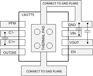
LM2775 layout.gifFigure 25. Example LM2775 Layout