ZHCSDQ0C March   2015  – August 2018 LP8758-B0

PRODUCTION DATA.  

  1. 特性
  2. 应用
  3. 说明
  4. 简化原理图
    1.     效率与输出电流 (VIN = 3.7V)
  5. 修订历史记录
  6. Pin Configuration and Functions
    1.     Pin Functions
  7. Specifications
    1. 7.1 Absolute Maximum Ratings
    2. 7.2 ESD Ratings
    3. 7.3 Recommended Operating Conditions
    4. 7.4 Thermal Information
    5. 7.5 Electrical Characteristics
    6. 7.6 I2C Serial Bus Timing Parameter
    7. 7.7 Switching Characteristics
    8. 7.8 Typical Characteristics
  8. Detailed Description
    1. 8.1 Overview
      1. 8.1.1 Buck Information
        1. 8.1.1.1 Operating Modes
        2. 8.1.1.2 Features
        3. 8.1.1.3 Programmability
    2. 8.2 Functional Block Diagram
    3. 8.3 Feature Description
      1. 8.3.1 Multi-Phase DC-DC Converters
        1. 8.3.1.1 Overview
        2. 8.3.1.2 Multi-Phase Operation and Phase Adding/Shedding
        3. 8.3.1.3 Transition Between PWM and PFM Modes
        4. 8.3.1.4 Multi-Phase Switcher Configurations
        5. 8.3.1.5 Buck Converter Load Current Measurement
        6. 8.3.1.6 Spread-Spectrum Mode
      2. 8.3.2 Power-Up
      3. 8.3.3 Regulator Control
        1. 8.3.3.1 Enabling and Disabling Regulator
        2. 8.3.3.2 Changing Output Voltage
      4. 8.3.4 Device Reset Scenarios
      5. 8.3.5 Diagnosis and Protection Features
        1. 8.3.5.1 Warnings for Diagnosis (Interrupt)
          1. 8.3.5.1.1 Output Current Limit
          2. 8.3.5.1.2 Thermal Warning
        2. 8.3.5.2 Protection (Regulator Disable)
          1. 8.3.5.2.1 Short-Circuit and Overload Protection
          2. 8.3.5.2.2 Thermal Shutdown
        3. 8.3.5.3 Fault (Power Down)
          1. 8.3.5.3.1 Undervoltage Lockout
      6. 8.3.6 Digital Signal Filtering
    4. 8.4 Device Functional Modes
      1. 8.4.1 Modes of Operation
    5. 8.5 Programming
      1. 8.5.1 I2C-Compatible Interface
        1. 8.5.1.1 Data Validity
        2. 8.5.1.2 Start and Stop Conditions
        3. 8.5.1.3 Transferring Data
        4. 8.5.1.4 I2C-Compatible Chip Address
        5. 8.5.1.5 Auto Increment Feature
    6. 8.6 Register Maps
      1. 8.6.1 Register Descriptions
        1. 8.6.1.1  DEV_REV
        2. 8.6.1.2  OTP_REV
        3. 8.6.1.3  BUCK0_CTRL1
        4. 8.6.1.4  BUCK0_CTRL2
        5. 8.6.1.5  BUCK1_CTRL2
        6. 8.6.1.6  BUCK2_CTRL2
        7. 8.6.1.7  BUCK3_CTRL2
        8. 8.6.1.8  BUCK0_VOUT
        9. 8.6.1.9  BUCK0_FLOOR_VOUT
        10. 8.6.1.10 BUCK0_DELAY
        11. 8.6.1.11 RESET
        12. 8.6.1.12 CONFIG
        13. 8.6.1.13 INT_TOP
        14. 8.6.1.14 INT_BUCK_0_1
        15. 8.6.1.15 INT_BUCK_2_3
        16. 8.6.1.16 TOP_STAT
        17. 8.6.1.17 BUCK_0_1_STAT
        18. 8.6.1.18 BUCK_2_3_STAT
        19. 8.6.1.19 TOP_MASK
        20. 8.6.1.20 BUCK_0_1_MASK
        21. 8.6.1.21 BUCK_2_3_MASK
        22. 8.6.1.22 SEL_I_LOAD
        23. 8.6.1.23 I_LOAD_2
        24. 8.6.1.24 I_LOAD_1
  9. Application and Implementation
    1. 9.1 Application Information
    2. 9.2 Typical Application
      1. 9.2.1 Design Requirements
      2. 9.2.2 Detailed Design Procedure
        1. 9.2.2.1 Application Components
          1. 9.2.2.1.1 Inductor Selection
          2. 9.2.2.1.2 Input Capacitor Selection
          3. 9.2.2.1.3 Output Capacitor Selection
      3. 9.2.3 Application Curves
  10. 10Power Supply Recommendations
  11. 11Layout
    1. 11.1 Layout Guidelines
    2. 11.2 Layout Example
  12. 12器件和文档支持
    1. 12.1 器件支持
      1. 12.1.1 第三方米6体育平台手机版_好二三四免责声明
    2. 12.2 文档支持
      1. 12.2.1 相关文档
    3. 12.3 接收文档更新通知
    4. 12.4 社区资源
    5. 12.5 商标
    6. 12.6 静电放电警告
    7. 12.7 术语表
  13. 13机械、封装和可订购信息

Output Current Limit

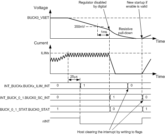
The buck regulators have programmable output peak current limits. The limits are individually programmed for all buck regulators with BUCKx_CTRL2.ILIMx[2:0] bits. The current limit settings of master and slave regulators used for the same output voltage rail must be identical. If the load current is increased so that the current limit is triggered, the regulator continues to regulate to the limit current level (current peak regulation). The voltage may decrease if the load current is higher than limit current. If the current regulation continues for 20 µs, the LP8758 device sets the INT_BUCKx.BUCKx_ILIM_INT bit and pulls the nINT pin low. The host processor can read BUCKx_STAT.BUCKx_ILIM_STAT bits to see if the regulator is still in peak current regulation mode.

If the load is so high that the output voltage decreases below a 350-mV level, the LP8758 device disables the regulator and sets the INT_BUCK_0_1.BUCK0_SC_INT bit. In addition the BUCK_0_1_STAT.BUCK0_STAT bit is set to 0. The interrupt is cleared when the host processor writes 1 to INT_BUCK_0_1.BUCK0_SC_INT bit. The overload situation is shown in Figure 13.
LP8758-B0 Overload_4ph.gifFigure 13. Overload Situation