ZHCSDQ0C March 2015 – August 2018 LP8758-B0
PRODUCTION DATA.
- 1 特性
- 2 应用
- 3 说明
- 4 简化原理图
- 5 修订历史记录
- 6 Pin Configuration and Functions
- 7 Specifications
-
8 Detailed Description
- 8.1 Overview
- 8.2 Functional Block Diagram
- 8.3 Feature Description
- 8.4 Device Functional Modes
- 8.5 Programming
- 8.6
Register Maps
- 8.6.1
Register Descriptions
- 8.6.1.1 DEV_REV
- 8.6.1.2 OTP_REV
- 8.6.1.3 BUCK0_CTRL1
- 8.6.1.4 BUCK0_CTRL2
- 8.6.1.5 BUCK1_CTRL2
- 8.6.1.6 BUCK2_CTRL2
- 8.6.1.7 BUCK3_CTRL2
- 8.6.1.8 BUCK0_VOUT
- 8.6.1.9 BUCK0_FLOOR_VOUT
- 8.6.1.10 BUCK0_DELAY
- 8.6.1.11 RESET
- 8.6.1.12 CONFIG
- 8.6.1.13 INT_TOP
- 8.6.1.14 INT_BUCK_0_1
- 8.6.1.15 INT_BUCK_2_3
- 8.6.1.16 TOP_STAT
- 8.6.1.17 BUCK_0_1_STAT
- 8.6.1.18 BUCK_2_3_STAT
- 8.6.1.19 TOP_MASK
- 8.6.1.20 BUCK_0_1_MASK
- 8.6.1.21 BUCK_2_3_MASK
- 8.6.1.22 SEL_I_LOAD
- 8.6.1.23 I_LOAD_2
- 8.6.1.24 I_LOAD_1
- 8.6.1
Register Descriptions
- 9 Application and Implementation
- 10Power Supply Recommendations
- 11Layout
- 12器件和文档支持
- 13机械、封装和可订购信息
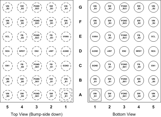
6 Pin Configuration and Functions
YFF Package
35-Pin DSBGA

Pin Functions
| PIN | TYPE | DESCRIPTION | |
|---|---|---|---|
| NUMBER | NAME | ||
| A1, B1 | VIN_B1 | P | Input for Buck 1. The separate power pins VIN_Bx are not connected together internally - VIN_Bx pins must be connected together in the application and be locally bypassed. |
| A2, B2 | SW_B1 | A | Buck 1 switch node. |
| A3, B3, C3 | PGND_B01 | G | Power Ground for Buck 0 and Buck 1. |
| A4, B4 | SW_B0 | A | Buck 0 switch node. |
| A5, B5 | VIN_B0 | P | Input for Buck 0. The separate power pins VIN_Bx are not connected together internally - VIN_Bx pins must be connected together in the application and be locally bypassed. |
| C1 | SGND | G | Substrate Ground. |
| C2 | FB_B1 | A | Output ground feedback (negative) for Buck 0. |
| C4 | FB_B0 | A | Output voltage feedback (positive) for Buck 0. |
| C5 | EN1 | D/I | Programmable Enable signal for Buck regulator. Can be also configured to switch between two output voltage levels. |
| D1 | AGND | G | Ground. |
| D2 | nINT | D/O | Open-drain interrupt output. Active LOW. |
| D3 | EN2 | D/I | Programmable Enable signal for Buck regulator. Can be also configured to switch between two output voltage levels. |
| D4 | NRST | D/I | Reset signal for the device. |
| D5 | SDA | D/I/O | Serial interface data input and output for system access. Connect a pull-up resistor. |
| E1 | VANA | P | Supply voltage for Analog and Digital blocks. VANA pin must be connected to same voltage as VIN_Bx pins. |
| E2 | FB_B3 | A | Output voltage feedback (positive) for Buck 3 - Connect to ground in 4-phase configuration. |
| E4 | FB_B2 | A | Output voltage feedback (positive) for Buck 2. - Connect to ground in 4-phase configuration. |
| E5 | SCL | D/I | Serial interface clock input for system access. Connect a pull-up resistor. |
| F1, G1 | VIN_B3 | P | Input for Buck 3. The separate power pins VIN_Bx are not connected together internally - VIN_Bx pins must be connected together in the application and be locally bypassed. |
| F2, G2 | SW_B3 | A | Buck 3 switch node. |
| E3, F3, G3 | PGND_B23 | G | Power Ground for Buck 2 and Buck 3. |
| F4, G4 | SW_B2 | A | Buck 2 switch node. |
| F5, G5 | VIN_B2 | P | Input for Buck 2. The separate power pins VIN_Bx are not connected together internally - VIN_Bx pins must be connected together in the application and be locally bypassed. |
| A: Analog Pin, D: Digital Pin, G: Ground Pin, P: Power Pin, I: Input Pin, O: Output Pin | |||