ZHCSDU0F May 2015 – March 2022 TUSB320
PRODUCTION DATA
- 1 特性
- 2 应用
- 3 说明
- 4 Revision History
- 5 Pin Configuration and Functions
- 6 Specifications
- 7 Detailed Description
- 8 Application and Implementation
- 9 Power Supply Recommendations
- 10Layout
- 11Device and Documentation Support
- 12Mechanical, Packaging, and Orderable Information
5 Pin Configuration and Functions
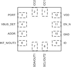
 Figure 5-1 RWB Package,12-Pin X2QFN(Top View)
Table 5-1 Pin Functions
| PIN | TYPE(3) | DESCRIPTION | |
|---|---|---|---|
| NAME | NO. | ||
| CC1 | 1 | I/O | Type-C configuration channel signal 1 |
| CC2 | 2 | I/O | Type-C configuration channel signal 2 |
| PORT(1) | 3 | I | Tri-level
input pin to indicate port mode. The state of this pin is sampled
when EN_N is asserted low and
VDD is active. This pin is also sampled following a I2C_SOFT_RESET.
H - DFP (Pull-up to VDD if DFP mode is desired) NC - DRP (Leave unconnected if DRP mode is desired) L - UFP (Pull-down or tie to GND if UFP mode is desired) |
| VBUS_DET(1) | 4 | I | 5- to 28-V VBUS input voltage. VBUS detection determines UFP attachment. One 900-kΩ external resistor required between system VBUS and VBUS_DET pin. |
| ADDR(1) | 5 | I | Tri-level
input pin to indicate I2C address or GPIO mode: H - I2C is enabled and I2C 7-bit address is 0x61. NC - GPIO mode (I2C is disabled) L - I2C is enabled and I2C 7-bit address is 0x60. ADDR pin should be pulled up to VDD if high configuration is desired |
| INT_N/OUT3(1) | 6 | O | The INT_N/OUT3 is a dual-function pin. When used as the INT_N, the pin is an open drain output in I2C control mode and is an active low interrupt signal for indicating changes in I2C registers. When used as OUT3, the pin is in audio accessory detect in GPIO mode: no detection (H), audio accessory connection detected (L). |
| SDA/OUT1(1)(2) | 7 | I/O | The SDA/OUT1 is a dual-function pin. When I2C is enabled (ADDR pin is high or low), this pin is the I2C communication data signal. When in GPIO mode (ADDR pin is NC), this pin is an open drain output for communicating Type-C current mode detect when the TUSB320 device is in UFP mode: Refer to Table 7-3 for more details. |
| SCL/OUT2(1)(2) | 8 | I/O | The SCL/OUT2 is a dual function pin. When I2C is enabled (ADDR pin is high or low), this pin is the I2C communication clock signal. When in GPIO mode (ADDR pin is NC), this pin is an open drain output for communicating Type-C current mode detect when the TUSB320 device is in UFP mode: Refer to Table 7-3 for more details. |
| ID(1) | 9 | O | Open drain output; asserted low when the CC pins detect device attachment when port is a source (DFP), or dual-role (DRP) acting as source (DFP). |
| GND | 10 | G | Ground |
| EN_N | 11 | I | Enable signal; active low. Pulled up to VDD internally to disable the TUSB320 device. If controlled externally, must be held high at least for 50 ms after VDD has reached its valid voltage level. |
| VDD | 12 | P | Positive supply voltage. VDD must ramp within 25 ms or less |
(1) When VDD is off, the
TUSB320 non-failsafe pins (VBUS_DET, ADDR, PORT, ID, OUT[3:1] pins) could
back-drive the TUSB320 device if not handled properly. When necessary to pull
these pins up, it is recommended to pullup PORT, ADDR, INT_N/OUT3, and ID to the
device VDD supply. The VBUS_DET must be pulled up to VBUS through a
900-kΩ resistor.
(2) When using the 3.3 V supply for
I2C, the end user must ensure that the VDD is 3 V and
above. Otherwise the I2C may back power the device.
(3) I = input, O = output, P = power