ZHCSDX8A June 2015 – June 2015 LM53602-Q1 , LM53603-Q1
PRODUCTION DATA.
- 1 特性
- 2 应用
- 3 说明
- 4 修订历史记录
- 5 Device Comparison Table
- 6 Pin Configuration and Functions
- 7 Specifications
- 8 Detailed Description
- 9 Application and Implementation
- 10Power Supply Recommendations
- 11Layout
- 12器件和文档支持
- 13机械、封装和可订购信息
11 Layout
11.1 Layout Guidelines
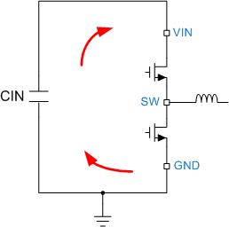
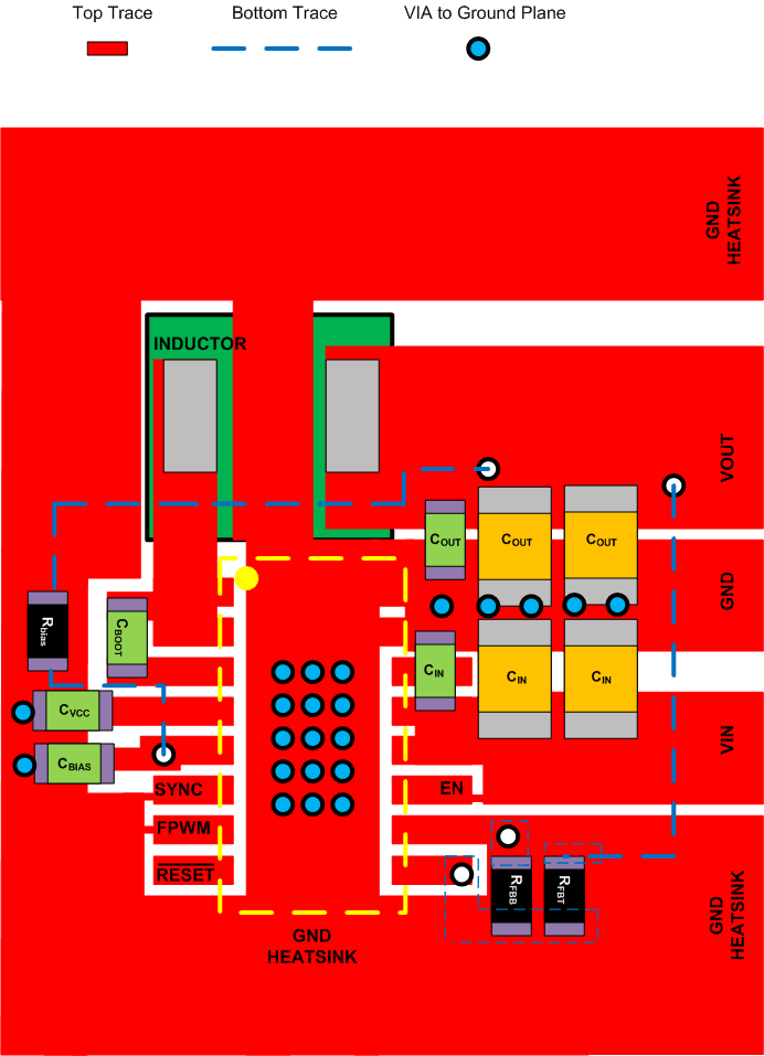
The PCB layout of any DC-DC converter is critical to the optimal performance of the design. Bad PCB layout can disrupt the operation of an otherwise good schematic design. Even if the converter regulates correctly, bad PCB layout can mean the difference between a robust design and one that cannot be mass produced. Furthermore, the EMI performance of the regulator is dependent on the PCB layout, to a great extent. In a buck converter, the most critical PCB feature is the loop formed by the input capacitor and power ground, as shown in Figure 44. This loop carries fast transient currents that can cause large transient voltages when reacting with the trace inductance. These unwanted transient voltages will disrupt the proper operation of the converter. Because of this, the traces in this loop should be wide and short, and the loop area as small as possible to reduce the parasitic inductance. Figure 45 shows a recommended layout for the critical components of the LM53603-Q1. This PCB layout is a good guide for any specific application. The following important guidelines should also be followed:
- Place the input capacitor(s) CIN as close as possible to the VIN and PGND terminals. VIN and GND are on the same side of the device, simplifying the input capacitor placement.
- Place bypass capacitors for VCC and BIAS close to their respective pins. These components must be placed close to the device and routed with short/wide traces to the pins and ground. The trace from BIAS to VOUT should be ≥10mils wide.
- Use wide traces for the CBOOT capacitor. CBOOT should be placed close to the device with short/wide traces to the CBOOT and SW pins.
- Place the feedback divider as close as possible to the FB pin on the device. If a feedback divider and CFF are used, they should be close to the device, while the length of the trace from VOUT to the divider can be somewhat longer. However, this latter trace should not be routed near any noise sources that can capacitively couple to the FB input.
- Use at least one ground plane in one of the middle layers. This plane will act as a noise shield and also act as a heat dissipation path.
- Connect the EP pad to the GND plane. This pad acts as a heat-sink connection and a ground connection for the regulator. It must be solidly connected to a ground plane. The integrity of this connection has a direct bearing on the effective RθJA.
- Provide wide paths for VIN, VOUT and GND. Making these paths as wide as possible reduces any voltage drops on the input or output paths of the converter and maximizes efficiency.
- Provide enough PCB area for proper heat-sinking. As stated in the Maximum Ambient Temperature section, enough copper area must be used to ensures a low RθJA, commensurate with the maximum load current and ambient temperature. The top and bottom PCB layers should be made with two ounce copper; and no less than one ounce. Use an array of heat-sinking vias to connect the exposed pad (EP) to the ground plane on the bottom PCB layer. If the PCB has multiple copper layers (recommended), these thermal vias can also be connected to the inner layer heat-spreading ground planes.
- Keep switch area small. The copper area connecting the SW pin to the inductor should be kept as short and wide as possible. At the same time the total area of this node should be minimized to help mitigate radiated EMI.
- The resources in Table 7 provide additional important guidelines
Table 7. PCB Layout Resources
| TITLE | LINK |
|---|---|
| AN-1149 Layout Guidelines for Switching Power Supplies | SNVA021 |
| AN-1229 Simple Switcher PCB Layout Guidelines | SNVA054 |
| Constructing Your Power Supply- Layout Considerations | SLUP230 |
| SNVA721 Low Radiated EMI Layout Made SIMPLE with LM4360x and LM4600x | SNVA721 |
 Figure 44. Current Loops with Fast Transients
11.1.1 Ground and Thermal Plane Considerations
As mentioned above, it is recommended to use one of the middle layers as a solid ground plane. A ground plane provides shielding for sensitive circuits and traces. It also provides a quiet reference potential for the control circuitry. The AGND and PGND pins should be connected to the ground plane using vias right next to the bypass capacitors. PGND pins are connected to the source of the internal low side MOSFET switch. They should be connected directly to the grounds of the input and output capacitors. The PGND net contains noise at the switching frequency and may bounce due to load variations. The PGND trace, as well as PVIN and SW traces, should be constrained to one side of the ground plane. The other side of the ground plane contains much less noise and should be used for sensitive routes.
It is recommended to provide adequate device heat sinking by utilizing the exposed pad (EP) of the IC as the primary thermal path. Use a minimum 4 by 4 array of 10 mil thermal vias to connect the EP to the system ground plane for heat sinking. The vias should be evenly distributed under the exposed pad. Use as much copper as possible for system ground plane on the top and bottom layers for the best heat dissipation. It is recommended to use a four-layer board with the copper thickness, starting from the top, as: 2 oz / 1 oz / 1 oz / 2 oz. A four layer board with enough copper thickness and proper layout provides low current conduction impedance, proper shielding and lower thermal resistance.
Table 8. Resources for Thermal PCB Design
| TITLE | LINK |
|---|---|
| AN-2020 Thermal Design By Insight, Not Hindsight | SNVA419 |
| AN-1520 A Guide to Board Layout for Best Thermal Resistance for Exposed Pad Packages | SNVA183 |
| SPRA953B Semiconductor and IC Package Thermal Metrics | SPRA953 |
| SNVA719 Thermal Design made Simple with LM43603 and LM43602 | SNVA719 |
| SLMA002 PowerPAD™ Thermally Enhanced Package | SLMA002 |
| SLMA004 PowerPAD Made Easy | SLMA004 |
| SBVA025 Using New Thermal Metrics | SBVA025 |
11.2 Layout Example
 Figure 45. PCB Layout Example