ZHCSE15F July 2015 – May 2018 SN65DP159 , SN75DP159
PRODUCTION DATA.
- 1 特性
- 2 应用
- 3 说明
- 4 修订历史记录
- 5 说明 (续)
- 6 Pin Configuration and Functions
-
7 Specifications
- 7.1 Absolute Maximum Ratings
- 7.2 ESD Ratings
- 7.3 Recommended Operating Conditions
- 7.4 Thermal Information
- 7.5 Power Supply Electrical Characteristics
- 7.6 Differential Input Electrical Characteristics
- 7.7 HDMI and DVI TMDS Output Electrical Characteristics
- 7.8 AUX, DDC, and I2C Electrical Characteristics
- 7.9 HPD Electrical Characteristics
- 7.10 HDMI and DVI Main Link Switching Characteristics
- 7.11 AUX Switching Characteristics (Only for RGZ Package)
- 7.12 HPD Switching Characteristics
- 7.13 DDC and I2C Switching Characteristics
- 7.14 Typical Characteristics
- 8 Parameter Measurement Information
-
9 Detailed Description
- 9.1 Overview
- 9.2 Functional Block Diagram
- 9.3
Feature Description
- 9.3.1 Reset Implementation
- 9.3.2 Operation Timing
- 9.3.3 I2C-over-AUX to DDC Bridge (SNx5DP159 48-Pin Package Version Only)
- 9.3.4 Input Lane Swap and Polarity Working
- 9.3.5 Main Link Inputs
- 9.3.6 Main Link Inputs Debug Tools
- 9.3.7 Receiver Equalizer
- 9.3.8 Termination Impedance Control
- 9.3.9 TMDS Outputs
- 9.4 Device Functional Modes
- 9.5 Register Maps
- 10Application and Implementation
- 11Power Supply Recommendations
- 12Layout
- 13器件和文档支持
- 14机械、封装和可订购信息
8 Parameter Measurement Information
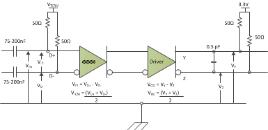 Figure 4. TMDS Main Link Test Circuit
 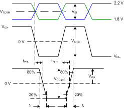 Figure 5. Input and Output Timing Measurements
 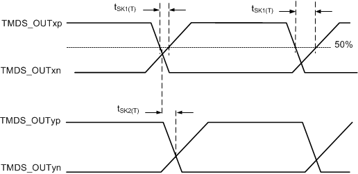 Figure 6. HDMI and DVI Sink TMDS Output Skew Measurements
  Figure 7. TMDS Main Link Common Mode Measurements
 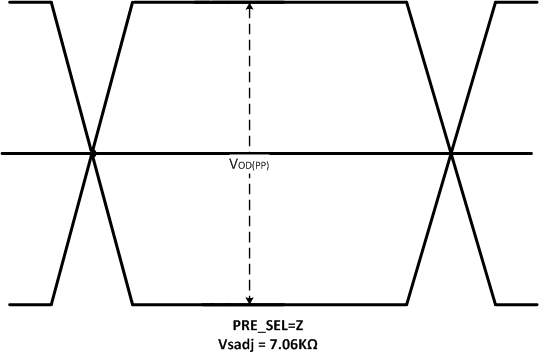 Figure 8. Output Differential Waveform 0 dB De-Emphasis
 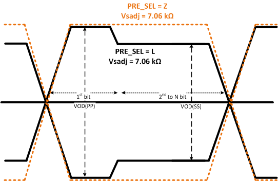 Figure 9. PRE_SEL = L for –2-dB De-Emphasis
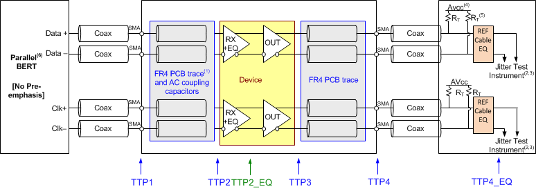
1. The FR4 trace between TTP1 and TTP2 is designed to emulate 1-8” of FR4, AC coupling cap, connector and another 1-2” of FR4. Trace width – 4 mils. 100-Ω differential impedance.
2. All jitter is measured at a BER of 10-9.
3. Residual jitter reflects the total jitter measured at TTP4 minus the jitter measured at TTP1.
4. AVCC = 3.3-V
5. RT = 50-Ω
6. The input signal from parallel bit error rate tester (BERT) does not have any pre-emphasis. Refer to Recommended Operating Conditions.
Figure 10. TMDS Output Jitter Measurement 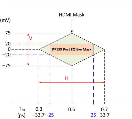 Figure 11. Post EQ Input Eye Mask at TTP2_EQ
 | TMDS DATA RATE (Gbps) | H (Tbit) | V (mV) |
| 3.4 < DR < 3.712 | 0.6 | 335 |
| 3.712 < DR < 5.94 | –0.0332Rbit2 + 0.2312Rbit + 0.1998 | –19.66Rbit2 + 106.74Rbit + 209.58 |
| 5.94 ≤ DR ≤ 6.0 | 0.4 | 150 |
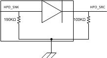 Figure 13. HPD Test Circuit
 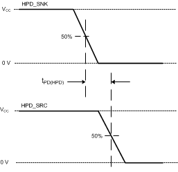 Figure 14. HPD Timing Diagram Number 1
 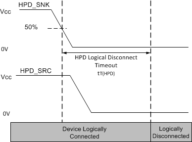 Figure 15. HPD Logic Disconnect Timeout
 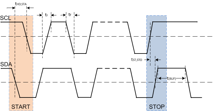 Figure 16. Start and Stop Condition Timing
 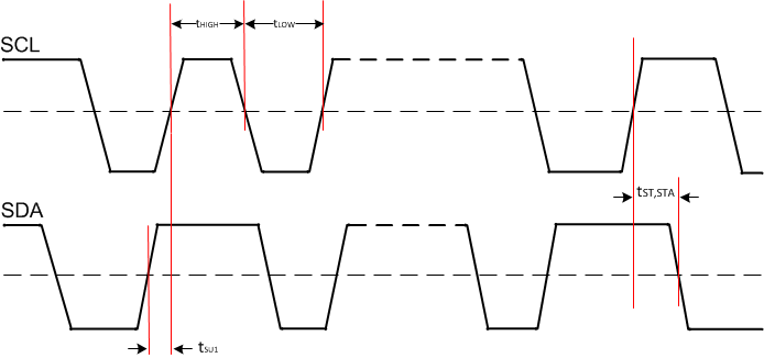 Figure 17. SCL and SDA Timing
 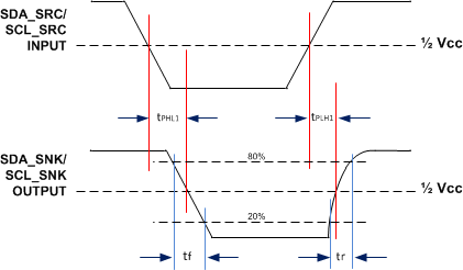 Figure 18. DDC Propagation Delay – Source to Sink
 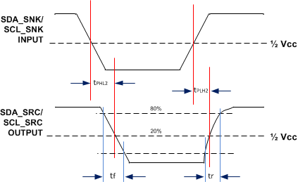 Figure 19. DDC Propagation Delay – Sink to Source