ZHCSE15F July 2015 – May 2018 SN65DP159 , SN75DP159
PRODUCTION DATA.
- 1 特性
- 2 应用
- 3 说明
- 4 修订历史记录
- 5 说明 (续)
- 6 Pin Configuration and Functions
-
7 Specifications
- 7.1 Absolute Maximum Ratings
- 7.2 ESD Ratings
- 7.3 Recommended Operating Conditions
- 7.4 Thermal Information
- 7.5 Power Supply Electrical Characteristics
- 7.6 Differential Input Electrical Characteristics
- 7.7 HDMI and DVI TMDS Output Electrical Characteristics
- 7.8 AUX, DDC, and I2C Electrical Characteristics
- 7.9 HPD Electrical Characteristics
- 7.10 HDMI and DVI Main Link Switching Characteristics
- 7.11 AUX Switching Characteristics (Only for RGZ Package)
- 7.12 HPD Switching Characteristics
- 7.13 DDC and I2C Switching Characteristics
- 7.14 Typical Characteristics
- 8 Parameter Measurement Information
-
9 Detailed Description
- 9.1 Overview
- 9.2 Functional Block Diagram
- 9.3
Feature Description
- 9.3.1 Reset Implementation
- 9.3.2 Operation Timing
- 9.3.3 I2C-over-AUX to DDC Bridge (SNx5DP159 48-Pin Package Version Only)
- 9.3.4 Input Lane Swap and Polarity Working
- 9.3.5 Main Link Inputs
- 9.3.6 Main Link Inputs Debug Tools
- 9.3.7 Receiver Equalizer
- 9.3.8 Termination Impedance Control
- 9.3.9 TMDS Outputs
- 9.4 Device Functional Modes
- 9.5 Register Maps
- 10Application and Implementation
- 11Power Supply Recommendations
- 12Layout
- 13器件和文档支持
- 14机械、封装和可订购信息
9.3.4 Input Lane Swap and Polarity Working
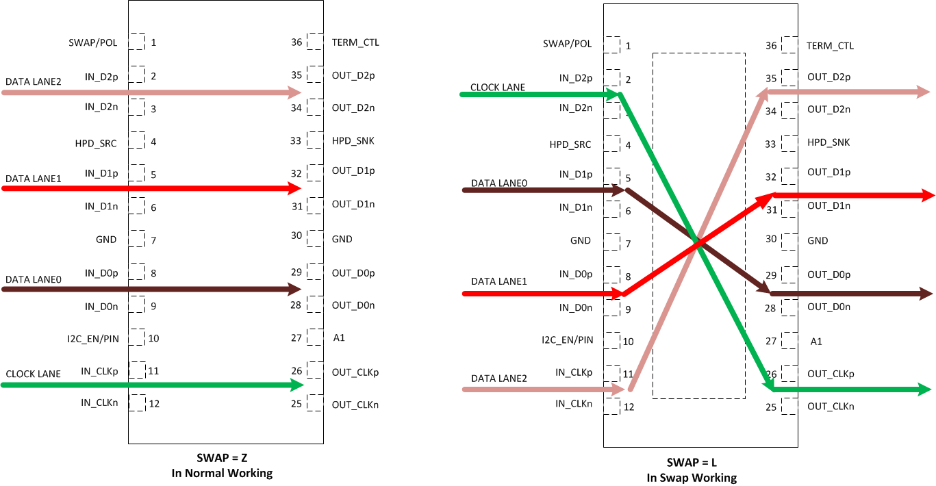
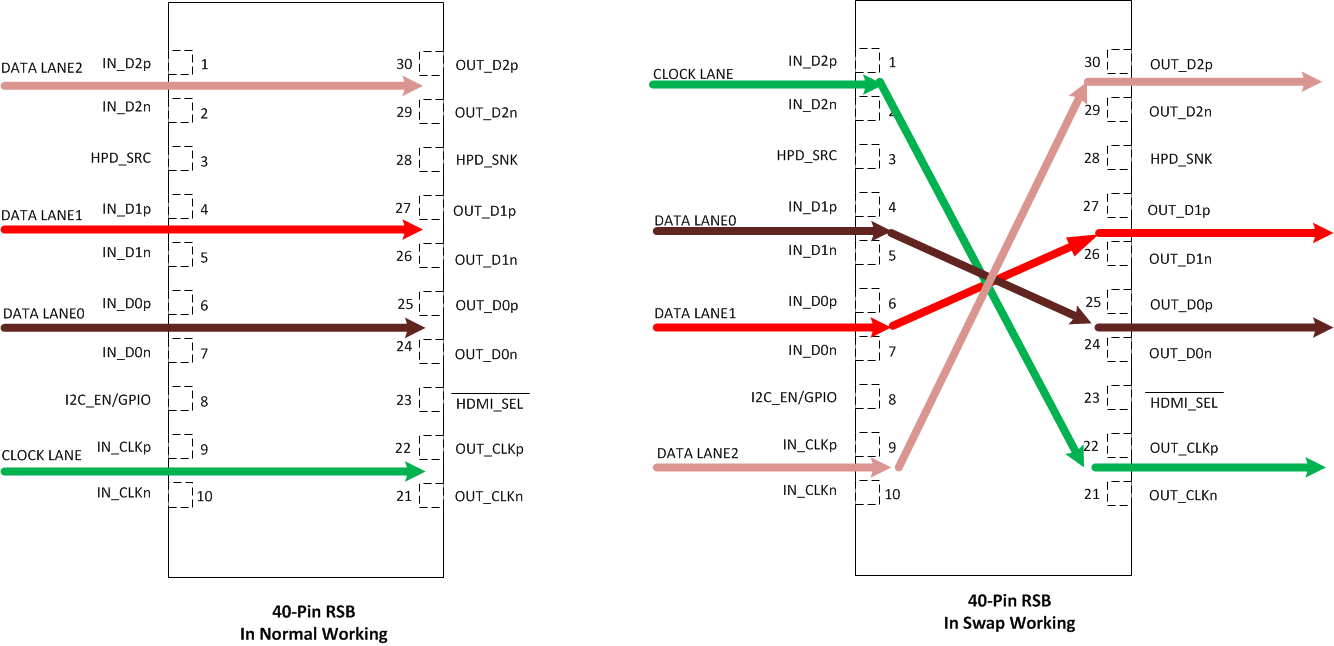
The SNx5DP159 device incorporates the swap function, which can set the input lanes in swap mode. The IN_D2 routes to the OUT_CLK position. The IN_D1 swaps with IN_D0. The swap function only changes the input pins; EQ setup follows new mapping. The SWAP/POL is pin 1 in the 48-pin RGZ package.For the RSB version, the user needs to control the register 0x09h bit 7 for SWAP enable. Lane swap is operational in both redriver and retimer mode.
Table 2. Lane Swap(1)
| NORMAL OPERATION | SWAP = L OR CSR 0x09h BIT 7 IS 1’b1 |
|---|---|
| IN_D2 → OUT_D2 | IN_D2 → OUT_CLK |
| IN_D1 → OUT_D1 | IN_D1 → OUT_D0 |
| IN_D0 → OUT_D0 | IN_D2 → OUT_D1 |
| IN_CLK → OUT_CLK | IN_CLK → OUT_D2 |
 Figure 24. SNx5DP159 Swap Function for 48 Pins
  Figure 25. SNx5DP159 Swap Function for 40 Pins
 The SNx5DP159 can also change the polarity of the input signals. When SWAP/POL is high, the n and p pins on each lane will swap.Use Register 0x9h bit 6 to swap polarity using I2C. Polarity swap only works for retimer mode. When the device is in automatic redriver to retimer mode this only works when device is in retimer stage. If set and data rate falls below 1.0-Gbps in this mode the polarity function will be lost.