ZHCSE15F July 2015 – May 2018 SN65DP159 , SN75DP159
PRODUCTION DATA.
- 1 特性
- 2 应用
- 3 说明
- 4 修订历史记录
- 5 说明 (续)
- 6 Pin Configuration and Functions
-
7 Specifications
- 7.1 Absolute Maximum Ratings
- 7.2 ESD Ratings
- 7.3 Recommended Operating Conditions
- 7.4 Thermal Information
- 7.5 Power Supply Electrical Characteristics
- 7.6 Differential Input Electrical Characteristics
- 7.7 HDMI and DVI TMDS Output Electrical Characteristics
- 7.8 AUX, DDC, and I2C Electrical Characteristics
- 7.9 HPD Electrical Characteristics
- 7.10 HDMI and DVI Main Link Switching Characteristics
- 7.11 AUX Switching Characteristics (Only for RGZ Package)
- 7.12 HPD Switching Characteristics
- 7.13 DDC and I2C Switching Characteristics
- 7.14 Typical Characteristics
- 8 Parameter Measurement Information
-
9 Detailed Description
- 9.1 Overview
- 9.2 Functional Block Diagram
- 9.3
Feature Description
- 9.3.1 Reset Implementation
- 9.3.2 Operation Timing
- 9.3.3 I2C-over-AUX to DDC Bridge (SNx5DP159 48-Pin Package Version Only)
- 9.3.4 Input Lane Swap and Polarity Working
- 9.3.5 Main Link Inputs
- 9.3.6 Main Link Inputs Debug Tools
- 9.3.7 Receiver Equalizer
- 9.3.8 Termination Impedance Control
- 9.3.9 TMDS Outputs
- 9.4 Device Functional Modes
- 9.5 Register Maps
- 10Application and Implementation
- 11Power Supply Recommendations
- 12Layout
- 13器件和文档支持
- 14机械、封装和可订购信息
10.1.1 Use Case of SNx5DP159
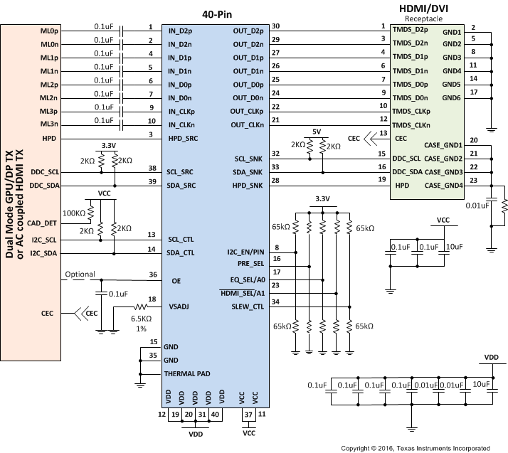
SNx5DP159 can be used on the motherboard and dongle applications. The following use case diagrams show the connection of AUX and DDC between source side and sink side. The control pin pull up and pull down resistors are shown from reference. If a high is needed only use the pull up. If a low is needed only use the pull down. If mid level is to be selected do not use either resistors and leave the pin floating/No connect. The 6.5-KΩ Vsadj resistor value shown is explained further in the compliance section, for the RSB package.
The DP159 was defined to work in mainly in source applications such as gaming systems, Blu-Ray DVD player, Desktop, Notebook or VR. The following sections provide design consideration for various types of applications.
Figure 30 shows the original connection of SNx5DP159 on motherboard through the DDC channel. The DDC DR default is 100-kHz and is capable to adjust to 400-kHz.
 Figure 30. Implementation for Motherboard 1
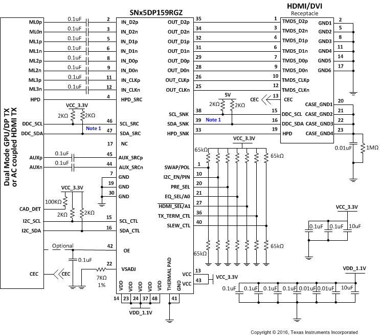
 Figure 31 shows the connection for both DDC and AUX GPU connections with the SNx5DP159RGZ. Only one can be implemented at a time. Only the RGZ package supports the I2C-over-AUX implementation. The control pin pull up and pull down resistors are shown for reference. If a high is needed only use the pull up. If a low is needed only use the pull down. If mid level is to be selected do not use either resistors and leave the pin floating/No connect.

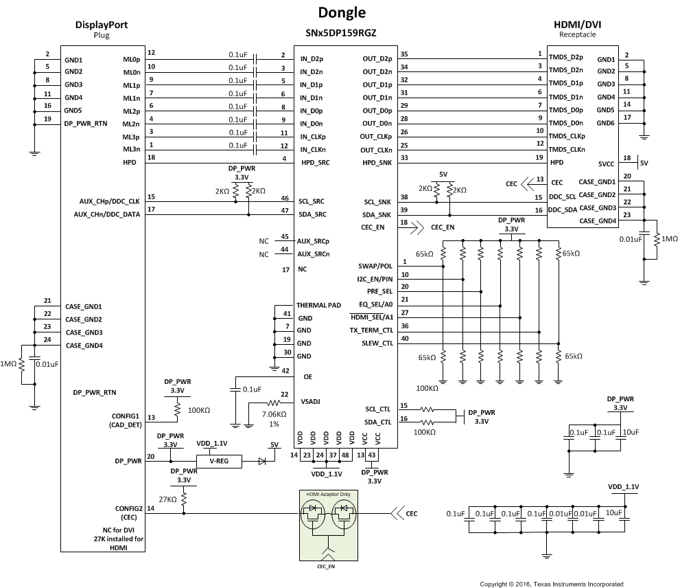
Figure 32 shows the SNx5DP159 in the dongle application. It uses the unified structure on DisplayPort connector. SNx5DP159 has to identify if the signal comes from DDC or from AUX in I2C-over-AUX format. Due to the AUX channel needed, use only the RGZ package for this application.
