ZHCSE42D April   2015  – April 2019 ADS54J60

PRODUCTION DATA.  

  1. 特性
  2. 应用
  3. 说明
    1.     170MHz 输入信号的 FFT
  4. 修订历史记录
  5. Device Comparison Table
  6. Pin Configuration and Functions
    1.     Pin Functions
  7. Specifications
    1. 7.1  Absolute Maximum Ratings
    2. 7.2  ESD Ratings
    3. 7.3  Recommended Operating Conditions
    4. 7.4  Thermal Information
    5. 7.5  Electrical Characteristics
    6. 7.6  AC Characteristics
    7. 7.7  Digital Characteristics
    8. 7.8  Timing Requirements
    9. 7.9  Typical Characteristics
    10. 7.10 Typical Characteristics: Contour
  8. Detailed Description
    1. 8.1 Overview
    2. 8.2 Functional Block Diagram
    3. 8.3 Feature Description
      1. 8.3.1 Analog Inputs
      2. 8.3.2 DDC Block
        1. 8.3.2.1 Decimate-by-2 Filter
        2. 8.3.2.2 Decimate-by-4 Filter Using a Digital Mixer
        3. 8.3.2.3 Decimate-by-4 Filter with IQ Outputs
      3. 8.3.3 SYSREF Signal
        1. 8.3.3.1 SYSREF Not Present (Subclass 0, 2)
      4. 8.3.4 Overrange Indication
        1. 8.3.4.1 Fast OVR
      5. 8.3.5 Power-Down Mode
    4. 8.4 Device Functional Modes
      1. 8.4.1 Device Configuration
        1. 8.4.1.1 Serial Interface
        2. 8.4.1.2 Serial Register Write: Analog Bank
        3. 8.4.1.3 Serial Register Readout: Analog Bank
        4. 8.4.1.4 JESD Bank SPI Page Selection
        5. 8.4.1.5 Serial Register Write: JESD Bank
          1. 8.4.1.5.1 Individual Channel Programming
        6. 8.4.1.6 Serial Register Readout: JESD Bank
      2. 8.4.2 JESD204B Interface
        1. 8.4.2.1 JESD204B Initial Lane Alignment (ILA)
        2. 8.4.2.2 JESD204B Test Patterns
        3. 8.4.2.3 JESD204B Frame
        4. 8.4.2.4 JESD204B Frame
        5. 8.4.2.5 JESD204B Frame Assembly with Decimation
          1. 8.4.2.5.1 JESD Transmitter Interface
          2. 8.4.2.5.2 Eye Diagram
    5. 8.5 Register Maps
      1. 8.5.1 Example Register Writes
      2. 8.5.2 Register Descriptions
        1. 8.5.2.1 General Registers
          1. 8.5.2.1.1 Register 0h (address = 0h)
            1. Table 20. Register 0h Field Descriptions
          2. 8.5.2.1.2 Register 1h (address = 1h)
            1. Table 21. Register 1h Field Descriptions
          3. 8.5.2.1.3 Register 2h (address = 2h)
            1. Table 22. Register 2h Field Descriptions
          4. 8.5.2.1.4 Register 3h (address = 3h)
            1. Table 23. Register 3h Field Descriptions
          5. 8.5.2.1.5 Register 4h (address = 4h)
            1. Table 24. Register 4h Field Descriptions
          6. 8.5.2.1.6 Register 5h (address = 5h)
            1. Table 25. Register 5h Field Descriptions
          7. 8.5.2.1.7 Register 11h (address = 11h)
            1. Table 26. Register 11h Field Descriptions
        2. 8.5.2.2 Master Page (080h) Registers
          1. 8.5.2.2.1  Register 20h (address = 20h), Master Page (080h)
            1. Table 27. Registers 20h Field Descriptions
          2. 8.5.2.2.2  Register 21h (address = 21h), Master Page (080h)
            1. Table 28. Register 21h Field Descriptions
          3. 8.5.2.2.3  Register 23h (address = 23h), Master Page (080h)
            1. Table 29. Register 23h Field Descriptions
          4. 8.5.2.2.4  Register 24h (address = 24h), Master Page (080h)
            1. Table 30. Register 24h Field Descriptions
          5. 8.5.2.2.5  Register 26h (address = 26h), Master Page (080h)
            1. Table 31. Register 26h Field Descriptions
          6. 8.5.2.2.6  Register 4Fh (address = 4Fh), Master Page (080h)
            1. Table 32. Register 4Fh Field Descriptions
          7. 8.5.2.2.7  Register 53h (address = 53h), Master Page (080h)
            1. Table 33. Register 53h Field Descriptions
          8. 8.5.2.2.8  Register 54h (address = 54h), Master Page (080h)
            1. Table 34. Register 54h Field Descriptions
          9. 8.5.2.2.9  Register 55h (address = 55h), Master Page (080h)
            1. Table 35. Register 55h Field Descriptions
          10. 8.5.2.2.10 Register 59h (address = 59h), Master Page (080h)
            1. Table 36. Register 59h Field Descriptions
        3. 8.5.2.3 ADC Page (0Fh) Register
          1. 8.5.2.3.1 Register 5F (address = 5F), ADC Page (0Fh)
            1. Table 37. Register 5F Field Descriptions
        4. 8.5.2.4 Main Digital Page (6800h) Registers
          1. 8.5.2.4.1  Register 0h (address = 0h), Main Digital Page (6800h)
            1. Table 38. Register 0h Field Descriptions
          2. 8.5.2.4.2  Register 41h (address = 41h), Main Digital Page (6800h)
            1. Table 39. Register 41h Field Descriptions
          3. 8.5.2.4.3  Register 42h (address = 42h), Main Digital Page (6800h)
            1. Table 41. Register 42h Field Descriptions
          4. 8.5.2.4.4  Register 43h (address = 43h), Main Digital Page (6800h)
            1. Table 42. Register 43h Field Descriptions
          5. 8.5.2.4.5  Register 44h (address = 44h), Main Digital Page (6800h)
            1. Table 43. Register 44h Field Descriptions
          6. 8.5.2.4.6  Register 4Bh (address = 4Bh), Main Digital Page (6800h)
            1. Table 44. Register 4Bh Field Descriptions
          7. 8.5.2.4.7  Register 4Dh (address = 4Dh), Main Digital Page (6800h)
            1. Table 45. Register 4Dh Field Descriptions
          8. 8.5.2.4.8  Register 4Eh (address = 4Eh), Main Digital Page (6800h)
            1. Table 46. Register 4Eh Field Descriptions
          9. 8.5.2.4.9  Register 52h (address = 52h), Main Digital Page (6800h)
            1. Table 47. Register 52h Field Descriptions
          10. 8.5.2.4.10 Register 72h (address = 72h), Main Digital Page (6800h)
            1. Table 48. Register 72h Field Descriptions
          11. 8.5.2.4.11 Register ABh (address = ABh), Main Digital Page (6800h)
            1. Table 49. Register ABh Field Descriptions
          12. 8.5.2.4.12 Register ADh (address = ADh), Main Digital Page (6800h)
            1. Table 50. Register ADh Field Descriptions
          13. 8.5.2.4.13 Register F7h (address = F7h), Main Digital Page (6800h)
            1. Table 51. Register F7h Field Descriptions
        5. 8.5.2.5 JESD Digital Page (6900h) Registers
          1. 8.5.2.5.1  Register 0h (address = 0h), JESD Digital Page (6900h)
            1. Table 52. Register 0h Field Descriptions
          2. 8.5.2.5.2  Register 1h (address = 1h), JESD Digital Page (6900h)
            1. Table 53. Register 1h Field Descriptions
          3. 8.5.2.5.3  Register 2h (address = 2h), JESD Digital Page (6900h)
            1. Table 55. Register 2h Field Descriptions
          4. 8.5.2.5.4  Register 3h (address = 3h), JESD Digital Page (6900h)
            1. Table 56. Register 3h Field Descriptions
          5. 8.5.2.5.5  Register 5h (address = 5h), JESD Digital Page (6900h)
            1. Table 57. Register 5h Field Descriptions
          6. 8.5.2.5.6  Register 6h (address = 6h), JESD Digital Page (6900h)
            1. Table 58. Register 6h Field Descriptions
          7. 8.5.2.5.7  Register 7h (address = 7h), JESD Digital Page (6900h)
            1. Table 59. Register 7h Field Descriptions
          8. 8.5.2.5.8  Register 16h (address = 16h), JESD Digital Page (6900h)
            1. Table 60. Register 16h Field Descriptions
          9. 8.5.2.5.9  Register 31h (address = 31h), JESD Digital Page (6900h)
            1. Table 61. Register 31h Field Descriptions
          10. 8.5.2.5.10 Register 32h (address = 32h), JESD Digital Page (6900h)
            1. Table 62. Register 32h Field Descriptions
        6. 8.5.2.6 JESD Analog Page (6A00h) Registers
          1. 8.5.2.6.1 Register 12h (address = 12h), JESD Analog Page (6A00h)
            1. Table 63. Register 12h-15h Field Descriptions
          2. 8.5.2.6.2 Registers 13h-15h (address = 13h-15h), JESD Analog Page (6A00h)
            1. Table 64. Register 13h-15h Field Descriptions
          3. 8.5.2.6.3 Register 16h (address = 16h), JESD Analog Page (6A00h)
            1. Table 65. Register 16h Field Descriptions
          4. 8.5.2.6.4 Register 17h (address = 17h), JESD Analog Page (6A00h)
            1. Table 66. Register 17h Field Descriptions
          5. 8.5.2.6.5 Register 1Ah (address = 1Ah), JESD Analog Page (6A00h)
            1. Table 67. Register 1Ah Field Descriptions
          6. 8.5.2.6.6 Register 1Bh (address = 1Bh), JESD Analog Page (6A00h)
            1. Table 68. Register 1Bh Field Descriptions
        7. 8.5.2.7 Offset Read Page (JESD BANK PAGE SEL = 6100h, JESD BANK PAGE SEL1 = 0000h) Registers
          1. 8.5.2.7.1 Register 068h (address = 068h), Offset Read Page
            1. Table 69. Register 068h Field Descriptions
          2. 8.5.2.7.2 Register 069h (address = 069h), Offset Read Page
            1. Table 70. Register 069h Field Descriptions
          3. 8.5.2.7.3 Registers 074h, 076h, 078h, 7Ah (address = 074h, 076h, 078h, 7Ah), Offset Read Page
            1. Table 71. Registers 074h, 076h, 078h, 7Ah Field Descriptions
          4. 8.5.2.7.4 Registers 075h, 077h, 079h, 7Bh (address = 075h, 077h, 079h, 7Bh), Offset Read Page
            1. Table 72. Registers 075h, 077h, 079h, 7Bh Field Descriptions
        8. 8.5.2.8 Offset Load Page (JESD BANK PAGE SEL= 6100h, JESD BANK PAGE SEL1 = 0500h) Registers
          1. 8.5.2.8.1 Registers 00h, 04h, 08h, 0Ch (address = 00h, 04h, 08h, 0Ch), Offset Load Page
            1. Table 73. Registers 00h, 04h, 08h, 0Ch Field Descriptions
          2. 8.5.2.8.2 Registers 01h, 05h, 09h, 0Dh (address = 01h, 05h, 09h, 0Dh), Offset Load Page
            1. Table 74. Registers 01h, 05h, 09h, 0Dh Field Descriptions
  9. Application and Implementation
    1. 9.1 Application Information
      1. 9.1.1 Start-Up Sequence
      2. 9.1.2 Hardware Reset
      3. 9.1.3 SNR and Clock Jitter
      4. 9.1.4 DC Offset Correction Block in the ADS54J60
        1. 9.1.4.1 Freezing the DC Offset Correction Block
        2. 9.1.4.2 Effect of Temperature
      5. 9.1.5 Idle Channel Histogram
    2. 9.2 Typical Application
      1. 9.2.1 Design Requirements
        1. 9.2.1.1 Transformer-Coupled Circuits
      2. 9.2.2 Detailed Design Procedure
      3. 9.2.3 Application Curves
  10. 10Power Supply Recommendations
    1. 10.1 Power Sequencing and Initialization
  11. 11Layout
    1. 11.1 Layout Guidelines
    2. 11.2 Layout Example
  12. 12器件和文档支持
    1. 12.1 文档支持
      1. 12.1.1 相关文档
    2. 12.2 接收文档更新通知
    3. 12.3 社区资源
    4. 12.4 商标
    5. 12.5 静电放电警告
    6. 12.6 术语表
  13. 13机械、封装和可订购信息

Timing Requirements

typical values are at TA = 25°C, full temperature range is from TMIN = –40°C to TMAX = 85°C, ADC sampling rate = 1.0 GSPS, 50% clock duty cycle, AVDD3V = 3.0 V, AVDD = DVDD = 1.9 V, IOVDD = 1.15 V, and –1-dBFS differential input (unless otherwise noted)
MIN TYP MAX UNITS
SAMPLE TIMING
Aperture delay 0.75 1.6 ns
Aperture delay matching between two channels on the same device ±70 ps
Aperture delay matching between two devices at the same temperature and supply voltage ±270 ps
Aperture jitter 120 fS rms
WAKE-UP TIMING
Wake-up time to valid data after coming out of global power-down 150 µs
LATENCY (1)
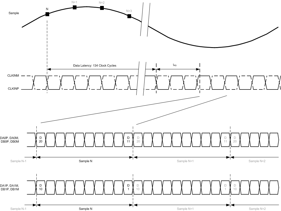
Data latency: ADC sample to digital output 134 Input clock cycles
OVR latency: ADC sample to OVR bit 62 Input clock cycles
FOVR latency: ADC sample to FOVR signal on pin 18 Input clock cycles
tPDI Propagation delay: logic gates and output buffers delay (does not change with fS) 4 ns
SYSREF TIMING
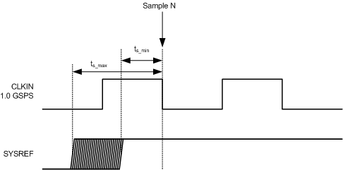
tSU_SYSREF Setup time for SYSREF, referenced to the input clock falling edge 300 900 ps
tH_SYSREF Hold time for SYSREF, referenced to the input clock falling edge 100 ps
JESD OUTPUT INTERFACE TIMING CHARACTERISTICS
Unit interval 100 400 ps
Serial output data rate 2.5 10 Gbps
Total jitter for BER of 1E-15 and lane rate = 10 Gbps 26 ps
Random jitter for BER of 1E-15 and lane rate = 10 Gbps 0.75 ps rms
Deterministic jitter for BER of 1E-15 and lane rate = 10 Gbps 12 ps, pk-pk
tR, tF Data rise time, data fall time: rise and fall times are measured from 20% to 80%,
differential output waveform, 2.5 Gbps ≤ bit rate ≤ 10 Gbps
35 ps
Overall latency = latency + tPDI.
ADS54J60 digital_characterstics_sbas706.gifFigure 1. SYSREF Timing
ADS54J60 timing_characterstics_sbas706.gifFigure 2. Sample Timing Requirements Diagram