ZHCSE42D April 2015 – April 2019 ADS54J60
PRODUCTION DATA.
- 1 特性
- 2 应用
- 3 说明
- 4 修订历史记录
- 5 Device Comparison Table
- 6 Pin Configuration and Functions
- 7 Specifications
-
8 Detailed Description
- 8.1 Overview
- 8.2 Functional Block Diagram
- 8.3 Feature Description
- 8.4 Device Functional Modes
- 8.5
Register Maps
- 8.5.1 Example Register Writes
- 8.5.2
Register Descriptions
- 8.5.2.1 General Registers
- 8.5.2.2
Master Page (080h) Registers
- 8.5.2.2.1 Register 20h (address = 20h), Master Page (080h)
- 8.5.2.2.2 Register 21h (address = 21h), Master Page (080h)
- 8.5.2.2.3 Register 23h (address = 23h), Master Page (080h)
- 8.5.2.2.4 Register 24h (address = 24h), Master Page (080h)
- 8.5.2.2.5 Register 26h (address = 26h), Master Page (080h)
- 8.5.2.2.6 Register 4Fh (address = 4Fh), Master Page (080h)
- 8.5.2.2.7 Register 53h (address = 53h), Master Page (080h)
- 8.5.2.2.8 Register 54h (address = 54h), Master Page (080h)
- 8.5.2.2.9 Register 55h (address = 55h), Master Page (080h)
- 8.5.2.2.10 Register 59h (address = 59h), Master Page (080h)
- 8.5.2.3 ADC Page (0Fh) Register
- 8.5.2.4
Main Digital Page (6800h) Registers
- 8.5.2.4.1 Register 0h (address = 0h), Main Digital Page (6800h)
- 8.5.2.4.2 Register 41h (address = 41h), Main Digital Page (6800h)
- 8.5.2.4.3 Register 42h (address = 42h), Main Digital Page (6800h)
- 8.5.2.4.4 Register 43h (address = 43h), Main Digital Page (6800h)
- 8.5.2.4.5 Register 44h (address = 44h), Main Digital Page (6800h)
- 8.5.2.4.6 Register 4Bh (address = 4Bh), Main Digital Page (6800h)
- 8.5.2.4.7 Register 4Dh (address = 4Dh), Main Digital Page (6800h)
- 8.5.2.4.8 Register 4Eh (address = 4Eh), Main Digital Page (6800h)
- 8.5.2.4.9 Register 52h (address = 52h), Main Digital Page (6800h)
- 8.5.2.4.10 Register 72h (address = 72h), Main Digital Page (6800h)
- 8.5.2.4.11 Register ABh (address = ABh), Main Digital Page (6800h)
- 8.5.2.4.12 Register ADh (address = ADh), Main Digital Page (6800h)
- 8.5.2.4.13 Register F7h (address = F7h), Main Digital Page (6800h)
- 8.5.2.5
JESD Digital Page (6900h) Registers
- 8.5.2.5.1 Register 0h (address = 0h), JESD Digital Page (6900h)
- 8.5.2.5.2 Register 1h (address = 1h), JESD Digital Page (6900h)
- 8.5.2.5.3 Register 2h (address = 2h), JESD Digital Page (6900h)
- 8.5.2.5.4 Register 3h (address = 3h), JESD Digital Page (6900h)
- 8.5.2.5.5 Register 5h (address = 5h), JESD Digital Page (6900h)
- 8.5.2.5.6 Register 6h (address = 6h), JESD Digital Page (6900h)
- 8.5.2.5.7 Register 7h (address = 7h), JESD Digital Page (6900h)
- 8.5.2.5.8 Register 16h (address = 16h), JESD Digital Page (6900h)
- 8.5.2.5.9 Register 31h (address = 31h), JESD Digital Page (6900h)
- 8.5.2.5.10 Register 32h (address = 32h), JESD Digital Page (6900h)
- 8.5.2.6
JESD Analog Page (6A00h) Registers
- 8.5.2.6.1 Register 12h (address = 12h), JESD Analog Page (6A00h)
- 8.5.2.6.2 Registers 13h-15h (address = 13h-15h), JESD Analog Page (6A00h)
- 8.5.2.6.3 Register 16h (address = 16h), JESD Analog Page (6A00h)
- 8.5.2.6.4 Register 17h (address = 17h), JESD Analog Page (6A00h)
- 8.5.2.6.5 Register 1Ah (address = 1Ah), JESD Analog Page (6A00h)
- 8.5.2.6.6 Register 1Bh (address = 1Bh), JESD Analog Page (6A00h)
- 8.5.2.7
Offset Read Page (JESD BANK PAGE SEL = 6100h, JESD BANK PAGE SEL1 = 0000h) Registers
- 8.5.2.7.1 Register 068h (address = 068h), Offset Read Page
- 8.5.2.7.2 Register 069h (address = 069h), Offset Read Page
- 8.5.2.7.3 Registers 074h, 076h, 078h, 7Ah (address = 074h, 076h, 078h, 7Ah), Offset Read Page
- 8.5.2.7.4 Registers 075h, 077h, 079h, 7Bh (address = 075h, 077h, 079h, 7Bh), Offset Read Page
- 8.5.2.8 Offset Load Page (JESD BANK PAGE SEL= 6100h, JESD BANK PAGE SEL1 = 0500h) Registers
- 9 Application and Implementation
- 10Power Supply Recommendations
- 11Layout
- 12器件和文档支持
- 13机械、封装和可订购信息
8.4.2 JESD204B Interface
The ADS54J60 supports device subclass 1 with a maximum output data rate of 10.0 Gbps for each serial transmitter.
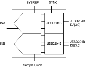
An external SYSREF signal is used to align all internal clock phases and the local multi-frame clock to a specific sampling clock edge, allowing synchronization of multiple devices in a system and minimizing timing and alignment uncertainty. The SYNC input is used to control the JESD204B SERDES blocks.
Depending on the ADC output data rate, the JESD204B output interface can be operated with either two or four lanes per single ADC; see Figure 76. The JESD204B setup and configuration of the frame assembly parameters is controlled via the SPI interface.
 Figure 76. ADS54J60 Block Diagram
 The JESD204B transmitter block shown in Figure 77 consists of the transport layer, the data scrambler, and the link layer. The transport layer maps the ADC output data into the selected JESD204B frame data format. The link layer performs the 8b/10b data encoding as well as the synchronization and initial lane alignment using the SYNC input signal. Optionally, data from the transport layer can be scrambled.
 Figure 77. JESD204B Transmitter Block