ZHCSE44C august 2015 – may 2023 ISO5852S
PRODUCTION DATA
- 1
- 1 特性
- 2 应用
- 3 说明
- 4 Revision History
- 5 说明(续)
- 6 Pin Configuration and Function
-
7 Specifications
- 7.1 Absolute Maximum Ratings
- 7.2 ESD Ratings
- 7.3 Recommended Operating Conditions
- 7.4 Thermal Information
- 7.5 Power Ratings
- 7.6 Insulation Specifications
- 7.7 Safety-Related Certifications
- 7.8 Safety Limiting Values
- 7.9 Electrical Characteristics
- 7.10 Switching Characteristics
- 7.11 Insulation Characteristics Curves
- 7.12 Typical Characteristics
- 8 Parameter Measurement Information
- 9 Detailed Description
-
10Application and Implementation
- 10.1 Application Information
- 10.2
Typical Applications
- 10.2.1 Design Requirements
- 10.2.2
Detailed Design Procedure
- 10.2.2.1 Recommended ISO5852S Application Circuit
- 10.2.2.2 FLT and RDY Pin Circuitry
- 10.2.2.3 Driving the Control Inputs
- 10.2.2.4 Local Shutdown and Reset
- 10.2.2.5 Global-Shutdown and Reset
- 10.2.2.6 Auto-Reset
- 10.2.2.7 DESAT Pin Protection
- 10.2.2.8 DESAT Diode and DESAT Threshold
- 10.2.2.9 Determining the Maximum Available, Dynamic Output Power, POD-max
- 10.2.2.10 Example
- 10.2.2.11 Higher Output Current Using an External Current Buffer
- 10.2.3 Application Curves
- 11Power Supply Recommendations
- 12Layout
- 13Device and Documentation Support
- 14Mechanical, Packaging, and Orderable Information
10.2.2.1 Recommended ISO5852S Application Circuit
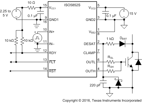
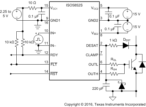
The ISO5852S device has both, inverting and noninverting gate-control inputs, an active-low reset input, and an open-drain fault output suitable for wired-OR applications. The recommended application circuit in Figure 10-2 shows a typical gate-driver implementation with unipolar output supply. Figure 10-3 shows a typical gate-driver implementation with bipolar output supply using the ISO5852S device.
A 0.1-μF bypass capacitor, recommended at the input supply pin VCC1, and 1-μF bypass capacitor, recommended at the VCC2 output supply pin, provide the large transient currents required during a switching transition to ensure reliable operation. The 220-pF blanking capacitor disables DESAT detection during the off-to-on transition of the power device. The DESAT diode (DDST) and the 1-kΩ series resistor on the DESAT pin are external protection components. The RG gate resistor limits the gate-charge current and indirectly controls the rise and fall times of the IGBT collector voltage. The open-drain
FLT output and RDY output have a passive
10-kΩ pullup resistor. In this application, the IGBT gate driver is disabled when a fault is detected and does not resume switching until the microcontroller applies a reset signal.
 Figure 10-2 Unipolar Output Supply
 Figure 10-3 Bipolar Output Supply