ZHCSE71I september 2015 – august 2023 SN6505A , SN6505B
PRODUCTION DATA
- 1
- 1 特性
- 2 应用
- 3 说明
- 4 Revision History
- 5 Pin Configuration and Functions
- 6 Specifications
- 7 Parameter Measurement Information
- 8 Detailed Description
- 9 Application and Implementation
- 10Power Supply Recommendations
- 11Layout
- 12Device and Documentation Support
- 13Mechanical, Packaging, and Orderable Information
9.1 Application Information
The SN6505 is a transformer driver designed for low-cost, small form-factor, isolated DC/DC converters using the push-pull topology. The device includes an oscillator that feeds a gate-drive circuit. The gate-drive, comprising a frequency divider and a break-before-make (BBM) logic, provides two complementary output signals which alternately turn the two output transistors on and off.
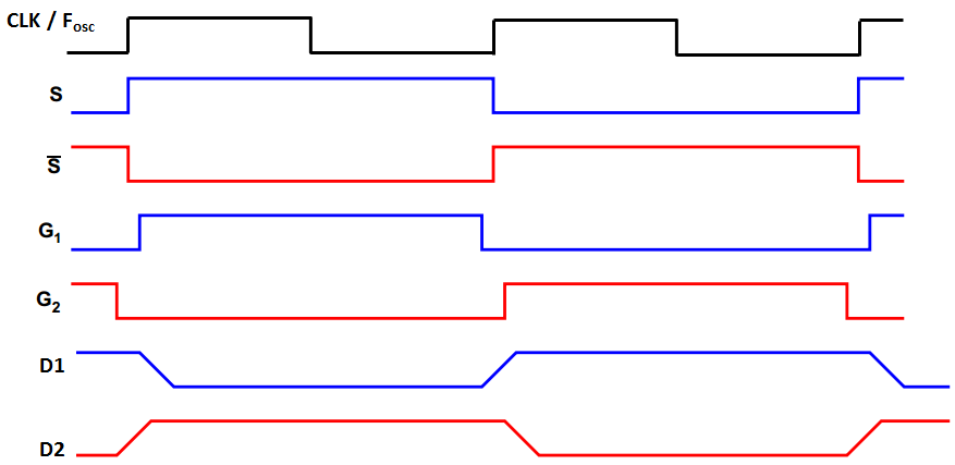
 Figure 9-1 Block Diagram and Output Timing With Break-Before-Make Action
The output frequency of the oscillator is divided down by an asynchronous divider that provides two complementary output signals, S and S, with a 50% duty cycle. A subsequent break-before-make logic inserts a dead-time between the high-pulses of the two signals. The resulting output signals, G1 and G2, present the gate-drive signals for the output transistors Q1 and Q2. As shown in Figure 9-2, before either one of the gates can assume logic high, there must be a short time period during which both signals are low and both transistors are high-impedance. This short period, known as break-before-make time, is required to avoid shorting out both ends of the primary.
 Figure 9-2 Detailed Output Signal Waveforms