ZHCSEG3C September 2015 – July 2016 SN65DP149 , SN75DP149
PRODUCTION DATA.
- 1 特性
- 2 应用
- 3 说明
- 4 修订历史记录
- 5 说明 (续)
- 6 Pin Configuration and Functions
-
7 Specifications
- 7.1 Absolute Maximum Ratings
- 7.2 ESD Ratings
- 7.3 Recommended Operating Conditions
- 7.4 Thermal Information
- 7.5 Power Supply Electrical Characteristics
- 7.6 Differential Input Electrical Characteristics
- 7.7 HDMI and DVI TMDS Output Electrical Characteristics
- 7.8 DDC, and I2C Electrical Characteristics
- 7.9 HPD Electrical Characteristics
- 7.10 HDMI and DVI Main Link Switching Characteristics
- 7.11 HPD Switching Characteristics
- 7.12 DDC and I2C Switching Characteristics
- 7.13 Typical Characteristics
- 8 Parameter Measurement Information
- 9 Detailed Description
- 10Application and Implementation
- 11Power Supply Recommendations
- 12Layout
- 13器件和文档支持
- 14机械、封装和可订购信息
10 Application and Implementation
NOTE
Information in the following applications sections is not part of the TI component specification, and TI does not warrant its accuracy or completeness. TI’s customers are responsible for determining suitability of components for their purposes. Customers should validate and test their design implementation to confirm system functionality.
10.1 Application Information
10.1.1 Use Case of SNx5DP149
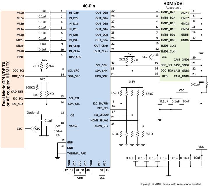
SNx5DP149 can be used on the motherboard and dongle applications. The following use case diagrams show the connection of DDC between source side and sink side. The control pin pull up and pull down resistors are shown from reference. If a high is needed only use the pull up. If a low is needed only use the pull down. If mid level is to be selected do not use either resistors and leave the pin floating/No connect. The 6.5-KΩ Vsadj resistor value shown is explained further in the compliance section.
Figure 28 shows the original connection of SNx5DP149 on motherboard through the DDC channel. The DDC DR default is 100-kHz and is capable to adjust to 400-kHz.
 Figure 28. Implementation for Motherboard
shows the SNx5DP149 in the dongle application. It uses the unified structure on DisplayPort connector.
10.1.2 DDC Pullup Resistors
NOTE
This section is for information only and subject to change depending upon system implementation.
The pullup resistor value is determined by two requirements:
- The maximum sink current of the I2C buffer:
The maximum sink current is 3-mA or slightly higher for an I2C driver supporting standard-mode I2C[4] operation. - The maximum transition time on the bus:
The maximum transition time, T, of an I2C bus is set by an RC time constant, where R is the pullup resistor value, and C is the total load capacitance. The parameter, k, can be calculated from Equation 3 by solving for t, the times at which certain voltage thresholds are reached. Different input threshold combinations introduce different values of t. Table 11 summarizes the possible values of k under different threshold combinations.


Table 11. Value k Upon Different Input Threshold Voltages
| Vth–\Vth+ | 0.7 VCC | 0.65 VCC | 0.6 VCC | 0.55 VCC | 0.5 VCC | 0.45 VCC | 0.4 VCC | 0.35 VCC | 0.3 VCC |
|---|---|---|---|---|---|---|---|---|---|
| 0.1 VCC | 1.0986 | 0.9445 | 0.8109 | 0.6931 | 0.5878 | 0.4925 | 0.4055 | 0.3254 | 0.2513 |
| 0.15 VCC | 1.0415 | 0.8873 | 0.7538 | 0.6360 | 0.5306 | 0.4353 | 0.3483 | 0.2683 | 0.1942 |
| 0.2 VCC | 0.9808 | 0.8267 | 0.6931 | 0.5754 | 0.4700 | 0.3747 | 0.2877 | 0.2076 | 0.1335 |
| 0.25 VCC | 0.9163 | 0.7621 | 0.6286 | 0.5108 | 0.4055 | 0.3102 | 0.2231 | 0.1431 | 0.0690 |
| 0.3 VCC | 0.8473 | 0.6931 | 0.5596 | 0.4418 | 0.3365 | 0.2412 | 0.1542 | 0.0741 |
From Equation 1, Rup(min) = 5.5-V / 3-mA = 1.83-kΩ to operate the bus under a 5-V pullup voltage and provide less than 3-mA when the I2C device is driving the bus to a low state. If a higher sink current, for example 4 mA, is allowed, Rup(min) can be as low as 1.375-kΩ.
If DDC is working at a standard mode of 100-Kbps, the maximum transition time, T, is fixed, 1 μs, and using the k values from Table 11, the recommended maximum total resistance of the pullup resistors on an I2C bus can be calculated for different system setups. If DDC is working in a fast mode of 400-kbps, the transition time should be set at 300 ns, according to I2C[4] specification.
To support the maximum load capacitance specified in the HDMI specification, Ccable(max) = 700-pF, Csource = 50-pF, Ci = 50-pF, and R(max) can be calculated as shown in Table 12.
Table 12. Pullup Resistor Upon Different Threshold Voltages and 800-pF Loads
| Vth–\Vth+ | 0.7 VCC | 0.65 VCC | 0.6 VCC | 0.55 VCC | 0.5 VCC | 0.45 VCC | 0.4 VCC | 0.35 VCC | 0.3 VCC | UNIT |
|---|---|---|---|---|---|---|---|---|---|---|
| 0.1 VCC | 1.14 | 1.32 | 1.54 | 1.8 | 2.13 | 2.54 | 3.08 | 3.84 | 4.97 | kΩ |
| 0.15 VCC | 1.2 | 1.41 | 1.66 | 1.97 | 2.36 | 2.87 | 3.59 | 4.66 | 6.44 | kΩ |
| 0.2 VCC | 1.27 | 1.51 | 1.8 | 2.17 | 2.66 | 3.34 | 4.35 | 6.02 | 9.36 | kΩ |
| 0.25 VCC | 1.36 | 1.64 | 1.99 | 2.45 | 3.08 | 4.03 | 5.6 | 8.74 | 18.12 | kΩ |
| 0.3 VCC | 1.48 | 1.8 | 2.23 | 2.83 | 3.72 | 5.18 | 8.11 | 16.87 | — | kΩ |
To accommodate the 3-mA drive current specification, a narrower threshold voltage range is required to support a maximum 800-pF load capacitance for a standard-mode I2C bus.
10.2 Typical Application
 Figure 29. Implementation for Motherboard Schematic
10.2.1 Design Requirements
The SNx5DP149 can be designed into many types of applications. All applications have certain requirements for the system to work properly. Two voltage rails are required to support the lowest possible power consumption. The OE pin must have a 0.1-µF capacitor to ground. This pin can be driven by a processor but the pin needs to change states after voltage rails have stabilized. Configure the device by using I2C. Pin strapping is provided as I2C is not available in all cases. Because sources may have different naming conventions, confirm the link between the source and the SNx5DP149 is correctly mapped. A swap function is provided for the input pins in case signaling is reversed between the source and the device. For the control pins the values provided below are when they are being controlled by a micro-controller. If this is not the case then using the 65-kΩ for a pull up for high, pulled down for low, and left floating for mid level.
Table 13. Design Parameters
| DESIGN PARAMETER | VALUE |
|---|---|
| VCC | 3.3 V |
| VDD | 1.1 V |
| Main link input voltage | VID = 75 mVpp to 1.2 Vpp |
| Control pin Low | 65-kΩ pulled to GND |
| Control pin Mid | No Connect |
| Control pin High | 65-kΩ pulled to 3.3-V |
| Vsadj resistor | 7.06-kΩ |
| Main link AC decoupling capacitor | 75 to 200 nF, recommend 100 nF |
10.2.2 Detailed Design Procedure
The SNx5DP149 is a signal conditioner that provides AC coupling to DC coupling level shifting, to support Dual Mode DisplayPort-capable GPUs or GPUs with AC-coupled drive capability to support HDMI or DVI connectors and compliance. Signal conditioning is accomplished using receive equalization, retiming, and output driver configurability. The transmitter drives 2 to 3 inches of board trace and connector.
Designing in the SNx5DP149 requires the following:
- Determine the loss profile between the GPU and the HDMI/DVI connector.
- Based upon the loss profile and signal swing, determine the optimal location for the SNx5DP149, to pass electrical compliance.
- Use the typical application drawings in Use Case of SNx5DP149 for information on using the AC coupling capacitors and control pin resistors.
- The DP149 has a receiver adaptive equalizer by default but can also be configured for fixed value equalization using the EQ_SEL control pin.
- Set the VOD, pre-emphasis, termination, and edge rate levels to support compliance by using the appropriate Vsadj resistor value and by setting the PRE_SEL and SLEW_CTL control pins.
- The thermal pad must be connected to ground.
- See the schematics in Application Information on recommended decouple capacitors from VCC pins to ground.
10.2.3 Application Curves
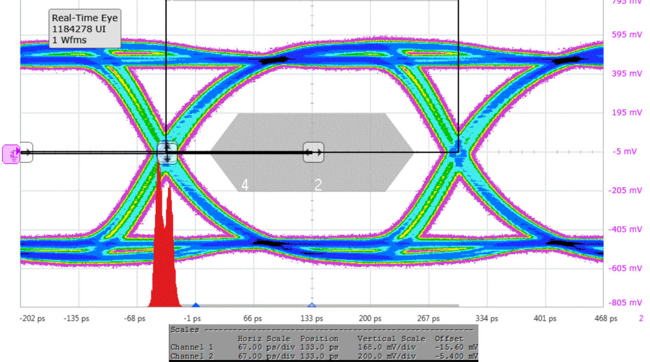
 Figure 30. 4k2k30 TX Compliance Eye
 Figure 31. 1080p TX Compliance Eye
10.3 System Example
10.3.1 Compliance Testing
Compliance testing is very system design specific. Properly designing the system and configuring the SNx5DP149 can help pass transmitter compliance for the system. The following information is the starting point to help prepare for compliance test. As each system is different there are many features in the DP149 to help tune the circuit. These include VOD adjust by changing the Vsadj resistor value or using I2C. Other knobs to turn are pre/de-emphasis and slew rate control. Passing HDMI1.4b compliance is easier to accomplish when using I2C as this provides more fine tuning capability.
For the SNx5DP149RSB:
Pin Strapping
HDMI1.4b
Vsadj Resistor = 6.5 kΩ
PRE_SEL = L for –2 dB
SLEW_CTL = NC
I2C
HDMI1.4b
Vsadj Resistor = 6.5 kΩ
VSWING_DATA & VSWING_CLK to -7% = Reg0Ch[7:2] = 111111
PRE_SEL = Reg0Ch[1:0] = 00: (Labeled HDMI_TWPST)
TX_TERM_CTL: Reg0Bh[4:3]
- <2 Gbps = 00 for no termination (This may be best value for all HDMI1.4b)
- >2 Gbps and < 3.4 Gbps = 01 for 150 to 300 Ω
SLEW_CTL = Reg0Bh[7:6] = 10