ZHCSEG6E December 2015 – December 2019 TCAN330 , TCAN330G , TCAN332 , TCAN332G , TCAN334 , TCAN334G , TCAN337 , TCAN337G
PRODUCTION DATA.
- 1 特性
- 2 应用
- 3 说明
- 4 修订历史记录
- 5 说明 (续)
- 6 Device Options
- 7 Pin Configuration and Functions
- 8 Specifications
- 9 Parameter Measurement Information
- 10Detailed Description
- 11Application and Implementation
- 12Power Supply Recommendations
- 13Layout
- 14器件和文档支持
- 15机械、封装和可订购信息
10.4.5 Bus Wake via RXD Request (BWRR) in Standby Mode
The TCAN334 with low power standby mode, offers a wake up from the CAN bus mechanism called bus wake via RXD Request (BWRR) to indicate to a host microprocessor that the bus is active and it should wake up and return to normal CAN communication.
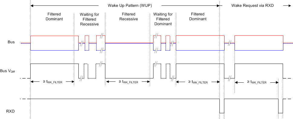
This device uses the multiple filtered dominant wake-up pattern (WUP) from ISO11898-5 to qualify bus traffic into a request to wake the host microprocessor. The bus wake request is signaled to the microprocessor by a falling edge and low corresponding to a “filtered” bus dominant on the RXD terminal (BWRR).
The wake up pattern (WUP) consists of a filtered dominant bus, then a filtered recessive bus time followed by a second filtered bus time. Once the WUP is detected the device will start issuing wake up requests (BWRR) on the RXD terminal every time a filtered dominant time is received from the bus. The first filtered dominant initiates the WUP and the bus monitor waits on a filtered recessive; other bus traffic does not reset the bus monitor. Once a filtered recessive is received, the bus monitor waits on a filtered dominant and again; other bus traffic does not reset the bus monitor. Immediately upon receiving of the second filtered dominant, the bus monitor recognizes the WUP and transitions to BWRR mode. In this mode, RXD is driven low for all dominant bits lasting for longer than tWK_FILTER. The RXD output during BWRR matches the classical 8-pin CAN devices, such as the TCANA1040A-Q1 device, that used the single filtered dominant on the bus as the wake up request mechanism from ISO11898-5.
For a dominant or recessive to be considered filtered, the bus must be in that state for more than tWK_FILTER time. Due to variability in the tWK_FILTER the following scenarios are applicable. Bus state times less than tWK_FILTER(MIN) are never detected as part of a WUP and thus no BWRR is generated. Bus state times between tWK_FILTER(MIN) and tWK_FILTER(MAX) may be detected as part of a WUP and a BWRR may be generated. Bus state times more than tWK_FILTER(MAX) are always detected as part of a WUP and thus a BWRR is always generated.
See Figure 33 for the timing diagram of the WUP. The pattern, tWK_FILTER time used for the WUP and BWRR prevent noise and bus stuck dominant faults from causing false wake requests. If the device is switched to normal mode, or an under voltage event occurs on VCC the BWRR will be lost.
 Figure 33. Wake Up Pattern (WUP) and Bus Wake via RXD Request (BWRR)