ZHCSEG6E December   2015  – December 2019 TCAN330 , TCAN330G , TCAN332 , TCAN332G , TCAN334 , TCAN334G , TCAN337 , TCAN337G

PRODUCTION DATA.  

  1. 特性
  2. 应用
  3. 说明
    1.     方框图
  4. 修订历史记录
  5. 说明 (续)
  6. Device Options
  7. Pin Configuration and Functions
    1.     Pin Functions
  8. Specifications
    1. 8.1 Absolute Maximum Ratings
    2. 8.2 ESD Ratings
    3. 8.3 Recommended Operating Conditions
    4. 8.4 Thermal Information
    5. 8.5 Electrical Characteristics
    6. 8.6 Switching Characteristics
    7. 8.7 Typical Characteristics
    8. 8.8 Typical Characteristics, TCAN330 Receiver
    9. 8.9 Typical Characteristics, TCAN330 Driver
  9. Parameter Measurement Information
  10. 10Detailed Description
    1. 10.1 Overview
    2. 10.2 Functional Block Diagram
    3. 10.3 Feature Description
      1. 10.3.1 TXD Dominant Timeout (TXD DTO)
      2. 10.3.2 RXD Dominant Timeout (RXD DTO)
      3. 10.3.3 Thermal Shutdown
      4. 10.3.4 Undervoltage Lockout and Unpowered Device
      5. 10.3.5 Fault Pin (TCAN337)
      6. 10.3.6 Floating Pins
      7. 10.3.7 CAN Bus Short Circuit Current Limiting
      8. 10.3.8 ESD Protection
      9. 10.3.9 Digital Inputs and Outputs
    4. 10.4 Device Functional Modes
      1. 10.4.1 CAN Bus States
      2. 10.4.2 Normal Mode
      3. 10.4.3 Silent Mode
      4. 10.4.4 Standby Mode with Wake
      5. 10.4.5 Bus Wake via RXD Request (BWRR) in Standby Mode
      6. 10.4.6 Shutdown Mode
      7. 10.4.7 Driver and Receiver Function Tables
  11. 11Application and Implementation
    1. 11.1 Application Information
      1. 11.1.1 Bus Loading, Length and Number of Nodes
    2. 11.2 Typical Application
      1. 11.2.1 Design Requirements
        1. 11.2.1.1 CAN Termination
      2. 11.2.2 Detailed Design Procedure
      3. 11.2.3 Application Curves
    3. 11.3 System Examples
      1. 11.3.1 ISO11898 Compliance of TCAN33x Family of 3.3-V CAN Transceivers Introduction
      2. 11.3.2 Differential Signal
      3. 11.3.3 Common-Mode Signal and EMC Performance
  12. 12Power Supply Recommendations
  13. 13Layout
    1. 13.1 Layout Guidelines
    2. 13.2 Layout Example
  14. 14器件和文档支持
    1. 14.1 相关链接
    2. 14.2 支持资源
    3. 14.3 商标
    4. 14.4 静电放电警告
    5. 14.5 Glossary
  15. 15机械、封装和可订购信息

Detailed Design Procedure

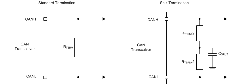
Termination is typically a 120-Ω resistor at each end of the bus. If filtering and stabilization of the common mode voltage of the bus is desired, then split termination may be used (see Figure 8). Split termination uses two 60-Ω resistors with a capacitor in the middle of these resistors to ground. Split termination improves the electromagnetic emissions behavior of the network by eliminating fluctuations in the bus common mode voltages at the start and end of message transmissions.

Care should be taken in the power ratings of the termination resistors used. Typically the worst case condition would be if the system power supply was shorted across the termination resistance to ground. In most cases the current flow through the resistor in this condition would be much higher than the transceiver's current limit.
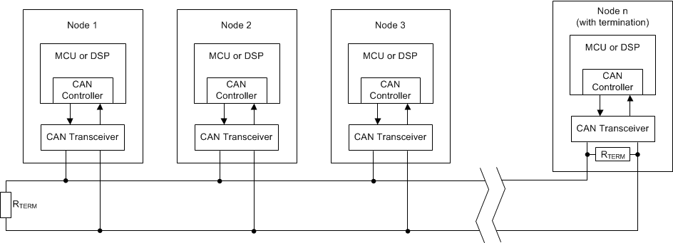
TCAN330 TCAN332 TCAN334 TCAN337 TCAN330G TCAN332G TCAN334G TCAN337G Typical_CAN_Bus_sllseq7.gifFigure 35. Typical CAN Bus
TCAN330 TCAN332 TCAN334 TCAN337 TCAN330G TCAN332G TCAN334G TCAN337G CAN_Bus_Termination_sllseq7.gifFigure 36. CAN Bus Termination Concepts