ZHCSEI2B January 2016 – June 2021 TPS7A84
PRODUCTION DATA
- 1 特性
- 2 应用
- 3 说明
- 4 Revision History
- 5 Pin Configurations and Functions
- 6 Specifications
- 7 Detailed Description
-
8 Application and Implementation
- 8.1
Application Information
- 8.1.1 Recommended Capacitor Types
- 8.1.2 Input and Output Capacitor Requirements (CIN and COUT)
- 8.1.3 Noise-Reduction and Soft-Start Capacitor (CNR/SS)
- 8.1.4 Feed-Forward Capacitor (CFF)
- 8.1.5 Soft-Start and In-Rush Current
- 8.1.6 Optimizing Noise and PSRR
- 8.1.7 Charge Pump Noise
- 8.1.8 ANY-OUT Programmable Output Voltage
- 8.1.9 ANY-OUT Operation
- 8.1.10 Increasing ANY-OUT Resolution for LILO Conditions
- 8.1.11 Current Sharing
- 8.1.12 Adjustable Operation
- 8.1.13 Sequencing Requirements
- 8.1.14 Power-Good Operation
- 8.1.15 Undervoltage Lockout (UVLO) Operation
- 8.1.16 Dropout Voltage (VDO)
- 8.1.17 Behavior when Transitioning from Dropout into Regulation
- 8.1.18 Load Transient Response
- 8.1.19 Negatively-Biased Output
- 8.1.20 Reverse Current Protection
- 8.1.21 Power Dissipation (PD)
- 8.1.22 Estimating Junction Temperature
- 8.1.23 Recommended Area for Continuous Operation (RACO)
- 8.2 Typical Applications
- 8.1
Application Information
- 9 Power Supply Recommendations
- 10Layout
- 11Device and Documentation Support
- 12Mechanical, Packaging, and Orderable Information
8.1.15 Undervoltage Lockout (UVLO) Operation
The UVLO circuit ensures that the device stays disabled before its input or bias supplies reach the minimum operational voltage range, and ensures that the device shuts down when the input supply or bias supply collapse.
The UVLO circuit has a minimum response time of several microseconds to fully assert. During this time, a downward line transient below approximately 0.8 V causes the UVLO to assert for a short time; however, the UVLO circuit does not have enough stored energy to fully discharge the internal circuits inside of the device. When the UVLO circuit does not fully discharge, the internal circuits of the output are not fully disabled.
The effect of the downward line transient can be mitigated by either using a larger input capacitor to limit the fall time of the input supply when operating near the minimum VIN, or by using a bias rail.
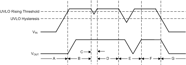
Figure 8-8 shows the UVLO circuit response to various input voltage events. The diagram can be separated into the following parts:
- Region A: The device does not turn on until the input reaches the UVLO rising threshold.
- Region B: Normal operation with a regulated output
- Region C: Brownout event above the UVLO falling threshold (UVLO rising threshold – UVLO hysteresis). The output may fall out of regulation but the device is still enabled.
- Region D: Normal operation with a regulated output
- Region E: Brownout event below the UVLO falling threshold. The device is disabled in most cases and the output falls because of the load and active discharge circuit. The device is reenabled when the UVLO rising threshold is reached by the input voltage and a normal start-up then follows.
- Region F: Normal operation followed by the input falling to the UVLO falling threshold.
- Region G: The device is disabled when the input voltage falls below the UVLO falling threshold to 0 V. The output falls because of the load and active discharge circuit.
 Figure 8-8 Typical UVLO Operation