ZHCSEK4E
December 2015 – August 2022
LMX2582
PRODUCTION DATA
1
特性
2
应用
3
说明
4
Revision History
5
Pin Configuration and Functions
6
Specifications
6.1
Absolute Maximum Ratings
6.2
ESD Ratings
6.3
Recommended Operating Conditions
6.4
Thermal Information
6.5
Electrical Characteristics
6.6
Timing Requirements
6.7
Typical Characteristics
7
Detailed Description
7.1
Overview
7.2
Functional Block Diagram
7.3
Functional Description
7.3.1
Input Signal
7.3.2
Input Signal Path
7.3.3
PLL Phase Detector and Charge Pump
7.3.4
N Divider and Fractional Circuitry
7.3.5
Voltage Controlled Oscillator
7.3.6
VCO Calibration
7.3.7
Channel Divider
7.3.8
Output Distribution
7.3.9
Output Buffer
7.3.10
Phase Adjust
7.4
Device Functional Modes
7.4.1
Power Down
7.4.2
Lock Detect
7.4.3
Register Readback
7.5
Programming
7.5.1
Recommended Initial Power on Programming Sequence
7.5.2
Recommended Sequence for Changing Frequencies
7.6
Register Maps
7.6.1
LMX2582 Register Map – Default Values
7.6.1.1
Register Descriptions
8
Application and Implementation
8.1
Application Information
8.1.1
Optimization of Spurs
8.1.1.1
Understanding Spurs by Offsets
8.1.1.2
Spur Mitigation Techniques
8.1.2
Configuring the Input Signal Path
8.1.2.1
Input Signal Noise Scaling
8.1.3
Input Pin Configuration
8.1.4
Using the OSCin Doubler
8.1.5
Using the Input Signal Path Components
8.1.5.1
Moving Phase Detector Frequency
8.1.5.2
Multiplying and Dividing by the Same Value
8.1.6
Designing for Output Power
8.1.7
Current Consumption Management
8.1.8
Decreasing Lock Time
8.1.9
Modeling and Understanding PLL FOM and Flicker Noise
8.1.10
External Loop Filter
8.2
Typical Application
8.2.1
Design for Low Jitter
8.2.1.1
Design Requirements
8.2.1.2
Detailed Design Procedure
8.2.1.3
Application Curve
8.3
Power Supply Recommendations
8.4
Layout
8.4.1
Layout Guidelines
8.4.2
Layout Example
9
Device and Documentation Support
9.1
Device Support
9.1.1
Development Support
9.2
Documentation Support
9.2.1
Related Documentation
9.3
接收文档更新通知
9.4
支持资源
9.5
Trademarks
9.6
Electrostatic Discharge Caution
9.7
术语表
10
Mechanical, Packaging, and Orderable Information
6.7
Typical Characteristics
T
A
= 25°C (unless otherwise noted)
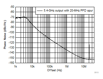
Figure 6-2
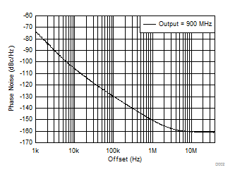
900-MHz Output - Closed-Loop Phase Noise
Figure 6-4
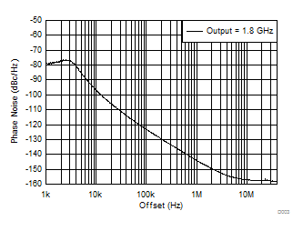
1.8-GHz Output - Closed-Loop Phase Noise
Figure 6-6
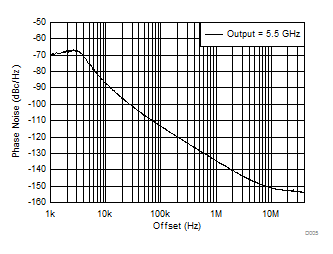
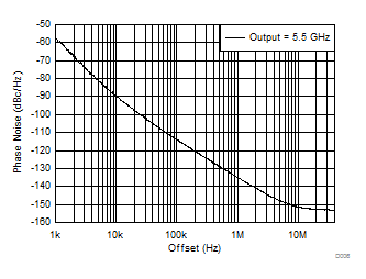
5.5-GHz Output - Closed-Loop Phase Noise
Figure 6-8
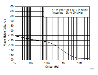
Integrated Jitter (47 fs) - 1.8-GHz Output
Figure 6-10
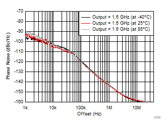
Variation of Phase Noise Across Temperature
Figure 6-12
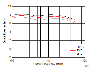
High Output Power (50-Ω Pullup, Single-Ended) vs Output Frequency
Figure 6-14
Typical PFD Spur for 5.4-GHz Output
Figure 6-16
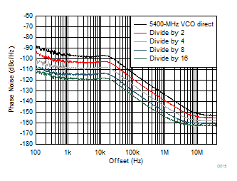
Impact of Channel Divider Settings on Phase Noise
Figure 6-3
900-MHz Output - Open-Loop Phase Noise
Figure 6-5
1.8-GHz Output - Open-Loop Phase Noise
Figure 6-7
5.5-GHz Output - Open-Loop Phase Noise
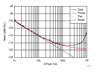
Figure 6-9
5.4-GHz Output Wide Loop Bandwidth – Showing PLL Performance
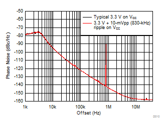
Figure 6-11
Impact of Supply Ripple on 1.8-GHz Output Phase Noise
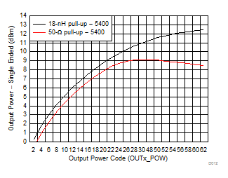
Figure 6-13
Output Power at 5.4-GHz Output vs OUTx_POW Code (1 - 31, 48 - 63)
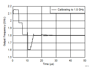
Figure 6-15
20-µs Frequency Change Time to 1.8 GHz With Fast Calibration
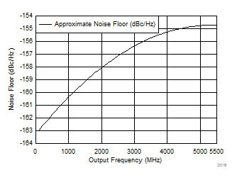
Figure 6-17
Noise Floor Variation With Output Frequency
千亿体育app官网登录(中国)官方网站IOS/安卓通用版/手机APP
|
米乐app下载官网(中国)|ios|Android/通用版APP最新版
|
米乐|米乐·M6(中国大陆)官方网站
|
千亿体育登陆地址
|
华体会体育(中国)HTH·官方网站
|
千赢qy国际_全站最新版千赢qy国际V6.2.14安卓/IOS下载
|
18新利网v1.2.5|中国官方网站
|
bob电竞真人(中国官网)安卓/ios苹果/电脑版【1.97.95版下载】
|
千亿体育app官方下载(中国)官方网站IOS/安卓/手机APP下载安装
|