ZHCSEQ1A February 2016 – February 2016 UCC28704
PRODUCTION DATA.
- 1 特性
- 2 应用
- 3 说明
- 4 修订历史记录
- 5 Pin Configuration and Functions
- 6 Specifications
-
7 Detailed Description
- 7.1 Overview
- 7.2 Functional Block Diagram
- 7.3
Feature Description
- 7.3.1 Detailed Pin Description
- 7.3.2 Primary-Side Regulation (PSR)
- 7.3.3 Primary-Side Constant Voltage (CV) Regulation
- 7.3.4 Primary-Side Constant Current (CC) Regulation
- 7.3.5 Valley-Switching and Valley-Skipping
- 7.3.6 Start-Up Operation
- 7.3.7 Fault Protection
- 7.3.8 Constant Current Under-Voltage Protection
- 7.3.9 Load Transient Response
- 7.4 Device Functional Modes
-
8 Applications and Implementation
- 8.1 Application Information
- 8.2
Typical Application
- 8.2.1 Design Requirements
- 8.2.2
Detailed Design Procedure
- 8.2.2.1 VDD Capacitance, CDD
- 8.2.2.2 VDD Start-Up Resistance, RSTR
- 8.2.2.3 Input Bulk Capacitance and Minimum Bulk Voltage
- 8.2.2.4 Transformer Turns Ratio, Inductance, Primary-Peak Current
- 8.2.2.5 Transformer Parameter Verification
- 8.2.2.6 VS Resistor Divider, Line Compensation, and NTC
- 8.2.2.7 Standby Power Estimate
- 8.2.2.8 Output Capacitance
- 8.2.2.9 Design Considerations in Using with Synchronous Rectifiers
- 8.2.3 Application Curves
- 8.3 Do's and Don'ts
- 9 Power Supply Recommendations
- 10Layout
- 11器件和文档支持
- 12机械、封装和可订购信息
8 Applications and Implementation
NOTE
Information in the following applications sections is not part of the TI component specification, and TI does not warrant its accuracy or completeness. TI’s customers are responsible for determining suitability of components for their purposes. Customers should validate and test their design implementation to confirm system functionality.
8.1 Application Information
The UCC28704 device is a PSR controller optimized for isolated-flyback AC-to-DC single-output supply applications, typically in the range from 5 W to 25 W, providing constant-voltage (CV) mode control and constant current (CC) mode control for precise output regulation; and to help meet USB-compliant adaptors and charger requirements as well as help meeting DOE Level VI or CoC V5 Tier 2 efficiency performance. The device uses the information obtained from auxiliary winding sensing (VS) to control the output voltage without requiring optocoupler/TL431 feedback circuitry. Not requiring optocoupler feedback reduces the component count and makes the design more cost effective.
8.2 Typical Application
Figure 24 illustrates a typical circuit diagram for AC-to-DC adapter applications. It is a flyback converter with primary-side regulation (PSR) controlled by UCC28704. Such applications widely exist in ac-dc adapters for smartphones, tablet-computers, and e-readers and so forth. The following sub-sections provide critical design formulas.
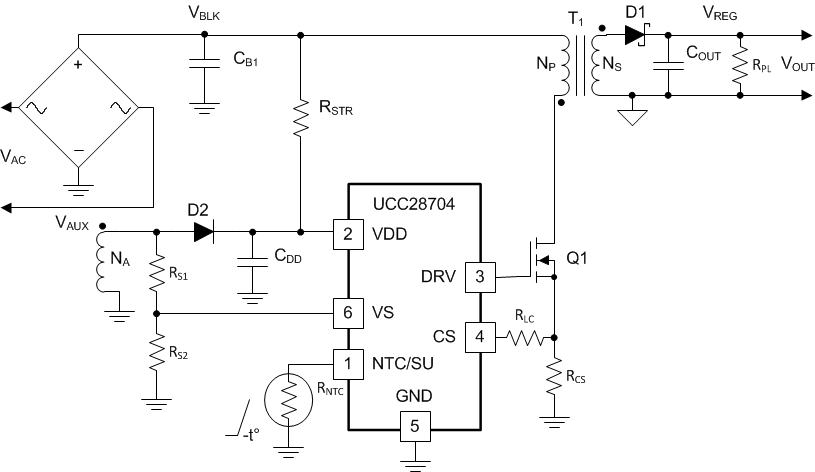 Figure 24. Typical Application Circuit
8.2.1 Design Requirements
The following table illustrates a typical subset of high-level design requirements for a particular converter of which many of the parameter values are used in the various design equations in this section. Many other necessary design parameters, such as fSW(MAX) and VBULK(min) for example, may not be listed in such a table. These values may be selected based on design experience or other considerations, and may be iterated to obtain optimal results.
Table 1. UCC28704 Design Parameters
| PARAMETER | TEST CONDITIONS | MIN | TYP | MAX | UNIT | |
|---|---|---|---|---|---|---|
| INPUT CHARACTERISTICS | ||||||
| VIN | AC-line input voltage | 85 | 115/230 | 265 | VRMS | |
| fLINE | Line frequency | 47 | 50/60 | 63 | Hz | |
| PSTBY | No-load input power | VIN = typ, IO = 0A | 43 | 50 | mW | |
| OUTPUT CHARACTERISTICS (MEASUREMENT AT 150-mΩ CABLE-END) | ||||||
| VO | DC output voltage | VIN = typ, IO = 0 to IOR | 4.75 | 5 | 5.25 | V |
| VRIPPLE | Output voltage ripple | VIN = typ, IO = IOR | 80 | mV | ||
| IOR | Output rated current | VIN = min to max | 2.0 | A | ||
| IOCC | Output constant current | VIN = typ, IO > IOR
2.7V < VO < 5V |
2.1 | 2.2 | 2.3 | A |
| VCCUV | CC UV shutdown interception | VIN= typ, IO = IOCC | 2.7 | V | ||
| ηAVG | Average efficiency | VIN= typ, average of 25%, 50%, 75%, and 100% Load | 80% | |||
| η10 | Light-load efficiency | VIN= typ, 10% load | 75% | |||
| SYSTEMS CHARACTERISTICS | ||||||
| fsw | Switching frequency | 1 | 65 | kHz | ||
| TON-Delay | Power-on delay time | VIN = min IO= IOR (constant resistor load) |
1.8 | s | ||
8.2.2 Detailed Design Procedure
This procedure outlines the steps to design a constant-voltage, constant-current flyback converter using the UCC28704 controller. Please refer to the Figure 24 for circuit details and section 器件命名规则 for variable definitions used in the applications equations below.
8.2.2.1 VDD Capacitance, CDD
The capacitance on VDD needs to supply the device operating current until the output of the converter reaches the target minimum operating voltage. At this time the auxiliary winding can sustain the voltage to the UCC28704. The total output current available to the load and to charge the output capacitors is the constant-current regulation target. The equation below assumes the output current of the flyback is available to charge the output capacitance until the minimum output voltage VOCC is achieved. The gate-drive current depends on particular MOSFET to be used. If with an estimated 1.0 mA of gate-drive current, CDD is determined by Equation 9.

8.2.2.2 VDD Start-Up Resistance, RSTR
Once the VDD capacitance is known, the start-up resistance from VBULK to achieve the power-on delay time (tSTR) target can be determined.

8.2.2.3 Input Bulk Capacitance and Minimum Bulk Voltage
Determine the minimum voltage on the input capacitance, CB1 and CB2 total, in order to determine the maximum Np to Ns turns ratio of the transformer. The input power of the converter based on target full-load efficiency, minimum input rms voltage, and minimum AC input frequency are used to determine the input capacitance requirement.
Maximum input power is determined based on VOCV, IOCC, and the full-load efficiency target. An initial estimate of 84% can be assumed for the full-load efficiency for a 5-V/2-A design.

Equation 12 provides an accurate solution for input capacitance based on a target minimum bulk capacitor voltage. To target a given input capacitance value, iterate the minimum capacitor voltage to achieve the target capacitance.

8.2.2.4 Transformer Turns Ratio, Inductance, Primary-Peak Current
The maximum primary-to-secondary turns ratio can be determined by the target maximum switching frequency at full load, the minimum input capacitor bulk voltage, and the estimated DCM resonant time.
Initially determine the maximum available total duty cycle of the on time and secondary conduction time based on target switching frequency and DCM resonant time. For DCM resonant time, assume 500 kHz if you do not have an estimate from previous designs. For the transition mode operation limit, the period required from the end of secondary current conduction to the first valley of the VDS voltage is ½ of the DCM resonant period, or 1 µs assuming 500-kHz resonant frequency. DMAX can be determined using Equation 13.

Once DMAX is known, the maximum turns ratio of the primary to secondary can be determined with the equation below. DMAGCC is defined as the secondary diode conduction duty cycle during constant-current, CC, operation. It is set internally by the UCC28704 at 0.475. The total voltage on the secondary winding needs to be determined; which is the sum of VOCV, the secondary rectifier VF, and the cable compensation voltage (VOCBC). For the 5-V USB charger applications, a turns ratio range of 12 to 15 is typically used for a 10-W design.

NPS is determined also with other design factors such as primary MOSFET, secondary rectifier diode, as well as secondary MOSFET if synchronous rectifier is used. Once an optimum turns-ratio is determined from a detailed transformer design, use this ratio for the following parameters.
The UCC28704 controller constant-current regulation is achieved by maintaining DMAGCC = 0.475 at the maximum primary current setting. The transformer turns ratio and constant-current regulating voltage determine the current sense resistor for a target constant current limit.
Since not all of the energy stored in the transformer is transferred to the secondary, a transformer efficiency term is included. This efficiency number includes the core and winding losses, leakage inductance ratio, and bias power ratio to rated output power. For a 5-V, 2-A charger example, bias power of 0.5% is a good estimate. An overall transformer efficiency of 94.5% is a good estimation of assuming 2% leakage inductance, 3% core and winding loss, and 0.5% bias power.
RCS is used to program the primary-peak current with Equation 15:

The primary transformer inductance can be calculated using the standard energy storage equation for flyback transformers. Primary current, maximum switching frequency, output and transformer efficiency are included in Equation 16. Initially determine transformer primary current.
Initially the transformer primary current should be determined. Primary current is simply the maximum current sense threshold divided by the current sense resistance.


The secondary winding to auxiliary winding transformer turns ratio (NAS) is determined by the lowest target operating output voltage in constant-current regulation and the VDD UVLO of the UCC28704. There is additional energy supplied to VDD from the transformer leakage inductance energy which allows a lower turns ratio to be used in many designs. The VOCC lower than CCUV level is not achievable because the CCUV protection is going to be triggered first.

8.2.2.5 Transformer Parameter Verification
The transformer turns-ratio selected affects the MOSFET VDS and secondary rectifier reverse voltage so these should be reviewed. The UCC28704 controller requires a minimum on time of the MOSFET (tON) and minimum DMAG time (tDMAG(min)) of the secondary rectifier in the high line, minimum-load condition. The selection of fMAX, LP and RCS affects the minimum tON and tDMAG.
The secondary rectifier and MOSFET voltage stress can be determined by the equations below.

For the MOSFET VDS voltage stress, an estimated leakage inductance voltage spike (VLK) needs to be included.

The following equations are used to determine for the minimum tON target of 0.3 µs and minimum de-mag time, tDMAG(min), target of 1.7 µs. The minimum tDMAG(min) target needs to be typically 2.45 µs when a synchronous rectifier is used on the secondary-side instead of a Schottky diode rectifier. Additional details are provided in Design Considerations in Using with Synchronous Rectifiers.


8.2.2.6 VS Resistor Divider, Line Compensation, and NTC
The VS divider resistors determine the output voltage regulation point of the flyback converter, also the high-side divider resistor (RS1) determines the line voltage at which the controller enables continuous DRV operation. RS1 is initially determined based on the transformer auxiliary to primary turns-ratio and the desired input voltage operating threshold.

The low-side VS pin resistor is selected based on desired VO regulation voltage. IVSL(run) is VS pin run current with a typical value 220 µA for a design.

The UCC28704 can maintain tight constant-current regulation over input line by utilizing the line compensation feature. The line compensation resistor (RLC) value is determined by current flowing in RS1 and expected gate drive and MOSFET turn-off delay. Assume a 50-ns internal delay in the UCC28704.

The NTC function on NTC/SU-pin is to program with a NTC resistor for the desired over-temperature shutdown threshold. The shut-down threshold is 0.95 V with an internal 105-μA current source which results in a 9.05-kΩ thermistor shut-down threshold. The SU function on NTC/SU-pin is described in Initial Power-On with A Depletion-Mode FET. Pulling down this pin to GND stops switching and can be used for remote enable and disable control. This pin should be left floating if not used.
8.2.2.7 Standby Power Estimate
Assuming no-load standby power is a critical design parameter, determine the estimated no-load power based on target converter maximum switching frequency and output power rating. The following equation estimates the stand-by power of the converter.

For a typical USB charger application, the bias power during no-load is approximately 2.1 mW. This is based on 21-V VDD and 100-µA bias current. The output preload resistor can be estimated by VOCV and the difference in the converter stand-by power and the bias power. The equation for output preload resistance accounts for bias power estimated at 2.1 mW. Preload resistor value is estimated in Equation 27 :

Typical start-up resistance values for RSTR range from 10 MΩ to 15 MΩ to achieve less than 2-s start-up time. The capacitor bulk voltage for the loss estimation is the highest voltage for the stand-by power measurement, typically 325 VDC.

For the total stand-by power estimation add an estimated 2.5 mW for snubber loss to the start-up resistance and converter stand-by power loss.

8.2.2.8 Output Capacitance
The output capacitance value is typically determined by the transient response requirement from no-load. For example, in some USB charger applications there is a requirement to maintain a minimum VO of 4.1 V with a load-step transient of 0 mA to 500 mA . Equation 30 assumes that the switching frequency can be at the UCC28704 minimum of fSW(min).

Equation 5 should be observed together with Equation 30 for stability consideration when determine COUT.
Another consideration of the output capacitor(s) is the ripple voltage requirement. The output capacitors and their total ESR are the main factors to determine the output voltage ripple. Equation 31 provides a formula to determine required ESR value RESR, and Equation 31 provides a formula to determine required capacitance. The total output ripple is the sum of these two parts with scale factors and 10mV to consider other noise as shown in Equation 33,


Example: if require VRIPPLE = 70 mV, assume 0.81 × VRIPPLE_R = 1.15 × VRIPPLE_C = 30 mV, then RESR = 4.05 mΩ, and COUT = 643 µF, with assumption of LP = 700 µH, IPP(max) = 0.713 A, NPS = 13, VOCV = 5 V, VCBC = 0.3 V.
8.2.2.9 Design Considerations in Using with Synchronous Rectifiers
Special design considerations need to be observed when using synchronous rectifiers (SR) with the UCC28704. Figure 14 depicts the de-mag time partition. When using UCC28704 with SR, a portion of the de-mag time needs to be reserved for tbw, as shown in Figure 25, which is the body diode conduction time when SR MOSFET turns off before the de-mag time ends.
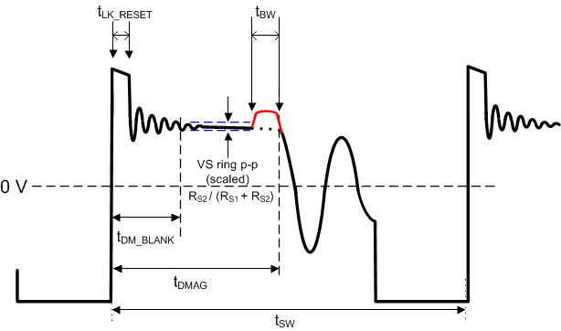 Figure 25. Auxiliary Waveform Details
The critical parameter dictating the maximum switching frequency when UCC28704 is used with an SR is determined based on tDMAG(min). The tDMAG(min) needs to be typically 2.45 µs including the SR bump width (tBW) is 750 ns. The 750-ns (tBW) is required for the internal circuit to filter out the SR bump change caused by MOSFET body diode conduction that is sensed on the VS pin waveform. The corresponding switching frequency measured at starting point of constant current operation should not be greater than 55 kHz.
8.2.3 Application Curves
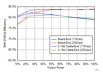
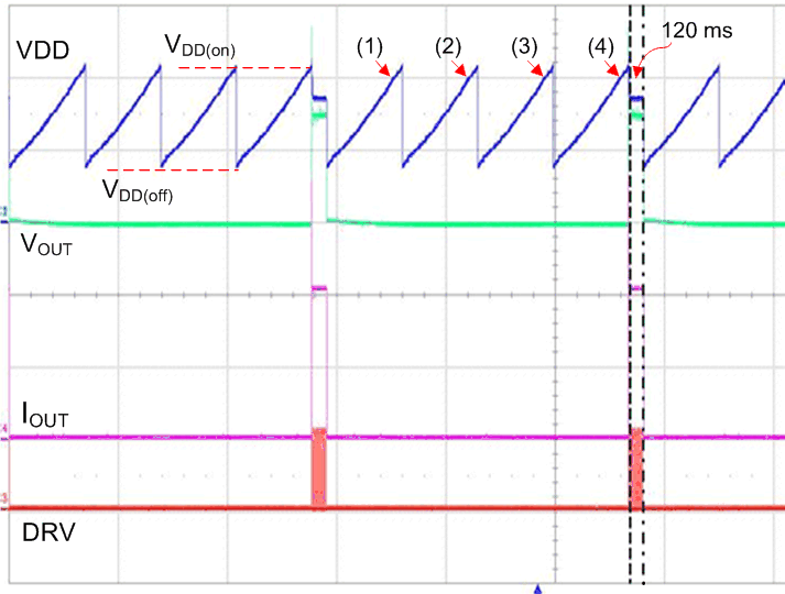
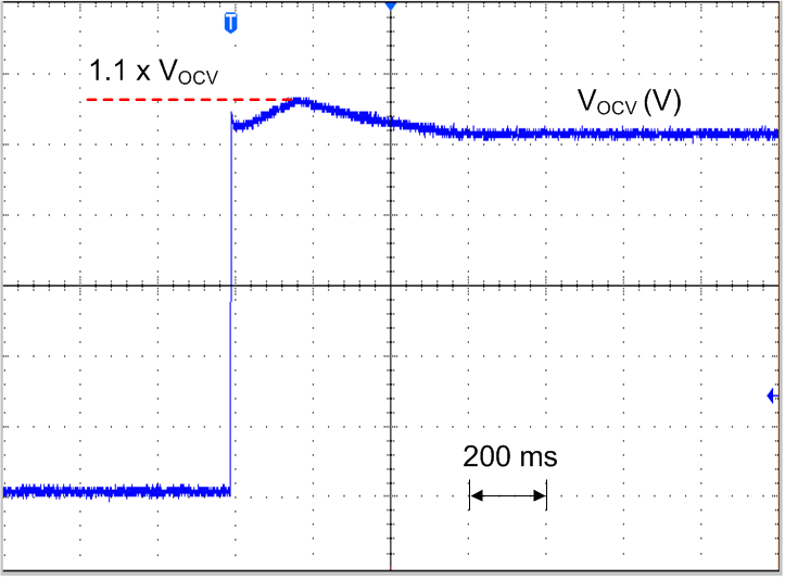
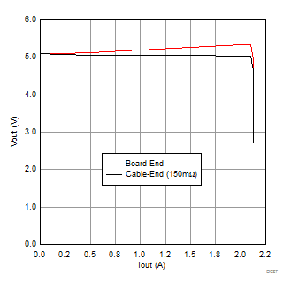
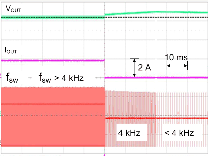
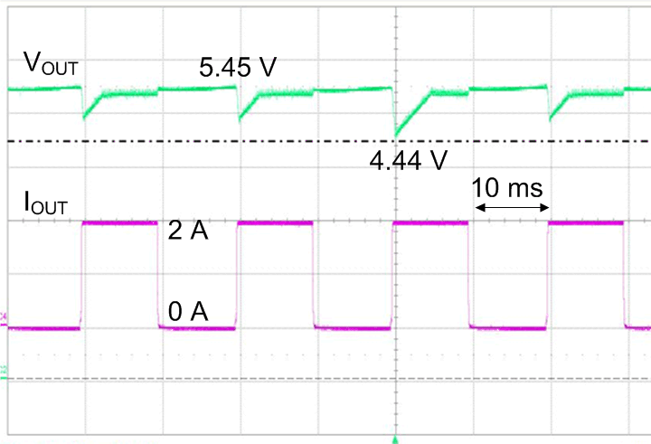
Figure 26 shows efficiency test result based on a 5-V/2-A, 10-W adapter using UCC28704. The efficiency performance exceeds CoC V5 Tier 2 (79% for average and 69.7% for a 10%-load) and DOE Level VI (78.7% for average) measured at 150-mΩ cable-end. As comparison, the measured result at board-end shown in Figure 26.
Figure 27 shows typical VI curves from the same 10-W board. The board-end output voltage has cable compensation to achieve cable-end output voltage with very well-regulated result in constant voltage mode operation range. In constant current mode operation, the result depicts a good constant current operation from the vertical line of current along with the output voltage drop until reaches CCUV. Notice that the CCUV difference at board-end and at cable-end is about 300 mV that is the same as cable compensation voltage at full load.
Figure 28 illustrates the timing diagram when the operation is in CCUV. The response of the controller to a soft-short circuit is shown wherein VOUT reaches to less than the VCCUV threshold. The converter is in CC mode and any additional load tending higher than IOCC causes VOUT to drop below regulation due to the soft-short. As VOUT is able to sustain VDD above its UVLO and the soft-short circuit condition persists continuously for 120 ms, the CCUV fault is initiated. The waveform shows the 3 VDD UVLO cycles that the controller goes through after the fault and it attempts to restart on the 4th VDD UVLO cycle with the response repeating due to the sustained soft short-circuit fault. The 120 ms is to blank any possible noise interference which may cause unnecessary CCUV protection to interrupt a normal operation.
Figure 29 provides the test result to explain the enhanced load transient scheme that is described in Load Transient Response. When the load steps down and demands a lower switching frequency, the controller clamps the switching frequency at 4 kHz until either the output has gone above its regulation level for more than 500 ms or has reached more than 10% of its VOCV. This enables the converter to have a better response to an ensuing load step up from the reduced response time. If either of the condition is met, then the controller starts to adjust the fSW below 4 kHz if the converter operation demands such a frequency.
Associated to this enhancement, the output voltage may experience a 10% overshoot as shown in Figure 29 during a load step-down or as shown in Figure 30 during a no-load start up.
Figure 31 shows the output load transient with load step change between 0-A and 2-A full load.
8.3 Do's and Don'ts
- During no-load operation, do allow sufficient margin for variations in VDD level to avoid the UVLO shutdown threshold. Also, at no-load, keep the average switching frequency greater than 1.5 × fSW(min) typical to avoid a rise in output voltage. RLC needs to be adjusted based on no-load operation accounting for both low-line and high-line operation..
- Do clean flux residue and contaminants from the PCB after assembly. Uncontrolled leakage current from VS to GND causes the output voltage to increase, while leakage current from VDD to VS can cause output voltage to increase.
- If ceramic capacitors are used for VDD, do use quality parts with X7R or X5R dielectric rated 50 V or higher to minimize reduction of capacitance due to DC-bias voltage and temperature variation.
- Do not use leaky components if low stand-by input power consumption is a design requirement.
- Do not probe the VS node with an ordinary oscilloscope probe; the probe capacitance can alter the signal and disrupt regulation.
- Do observe VS indirectly by probing the auxiliary winding voltage at RS1 and scaling the waveform by the VS divider ratio.
- Do follow Equation 5, Equation 30, Equation 31 to Equation 33 for COUT.