ZHCSEQ1A February 2016 – February 2016 UCC28704
PRODUCTION DATA.
- 1 特性
- 2 应用
- 3 说明
- 4 修订历史记录
- 5 Pin Configuration and Functions
- 6 Specifications
-
7 Detailed Description
- 7.1 Overview
- 7.2 Functional Block Diagram
- 7.3
Feature Description
- 7.3.1 Detailed Pin Description
- 7.3.2 Primary-Side Regulation (PSR)
- 7.3.3 Primary-Side Constant Voltage (CV) Regulation
- 7.3.4 Primary-Side Constant Current (CC) Regulation
- 7.3.5 Valley-Switching and Valley-Skipping
- 7.3.6 Start-Up Operation
- 7.3.7 Fault Protection
- 7.3.8 Constant Current Under-Voltage Protection
- 7.3.9 Load Transient Response
- 7.4 Device Functional Modes
-
8 Applications and Implementation
- 8.1 Application Information
- 8.2
Typical Application
- 8.2.1 Design Requirements
- 8.2.2
Detailed Design Procedure
- 8.2.2.1 VDD Capacitance, CDD
- 8.2.2.2 VDD Start-Up Resistance, RSTR
- 8.2.2.3 Input Bulk Capacitance and Minimum Bulk Voltage
- 8.2.2.4 Transformer Turns Ratio, Inductance, Primary-Peak Current
- 8.2.2.5 Transformer Parameter Verification
- 8.2.2.6 VS Resistor Divider, Line Compensation, and NTC
- 8.2.2.7 Standby Power Estimate
- 8.2.2.8 Output Capacitance
- 8.2.2.9 Design Considerations in Using with Synchronous Rectifiers
- 8.2.3 Application Curves
- 8.3 Do's and Don'ts
- 9 Power Supply Recommendations
- 10Layout
- 11器件和文档支持
- 12机械、封装和可订购信息
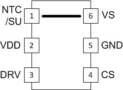
5 Pin Configuration and Functions
SOT23-6 Package
6-Pin DBV
Top View

Pin Functions
| PIN | I/O(1) | DESCRIPTION | ||
|---|---|---|---|---|
| NAME | NO. | |||
| NTC/SU | 1 | I/O | NTC/SU is a multi-function pin. First, it provides an interface to an external NTC (negative temperature coefficient) resistor for remote temperature sensing. Pulling this pin low shuts down PWM action. Additionally, when used with an external depletion-mode FET and a low-voltage NPN transistor this pin provides high-voltage start up control. A maximum 100-pF noise filter capacitance may be added to this pin. The pin should be left floating if not used. | |
| VDD | 2 | P | VDD is the bias supply input pin to the device. | |
| DRV | 3 | O | DRV is an output pin used to drive the gate of an external high voltage MOSFET switching transistor. | |
| CS | 4 | I | CS input connects to a ground referenced current sense resistor in series with the power switch. The resulting voltage is used to monitor and control the peak-primary current. A series resistor is added to this pin to compensate the peak-primary current levels as the AC mains input varies. A small capacitance, up to 30 pF, can be added to this pin to filter the current sense signal. | |
| GND | 5 | G | GND pin is both the reference pin for the controller and the low-side return for the drive output. Special care should be taken to return all AC decoupling capacitors as close as possible to this pin and avoid any common-mode signal trace length with analog signal return paths. | |
| VS | 6 | I | VS is an input used to provide voltage and timing feedback to the controller. This pin is connected to a voltage divider between an auxiliary winding and GND. The value of the upper resistor of this divider is used to program the AC-mains run-and-stop thresholds and line compensation at the CS pin. Avoid placing a filter capacitor on this input which would interfere with accurate sensing of this waveform. | |
(1)